SLES211C February 2008 – July 2015 PCM1681 , PCM1681-Q1
PRODUCTION DATA.
- 1 Features
- 2 Applications
- 3 Description
- 4 Revision History
- 5 Description (continued)
- 6 Pin Configuration and Functions
- 7 Specifications
-
8 Detailed Description
- 8.1 Overview
- 8.2 Functional Block Diagram
- 8.3 Feature Description
- 8.4 Device Functional Modes
- 8.5 Programming
- 8.6
Register Maps
- 8.6.1 Reserved Registers
- 8.6.2
Register Definitions
- 8.6.2.1 ATx[7:0]: Digital Attenuation Level Setting
- 8.6.2.2 MUTx: Soft Mute Control
- 8.6.2.3 DACx: DAC Operation Control
- 8.6.2.4 FLT: Digital Filter Roll-Off Control
- 8.6.2.5 FMT[3:0]: Audio Interface Data Format
- 8.6.2.6 SRST: Reset
- 8.6.2.7 ZREV: Zero-Flag Polarity Select
- 8.6.2.8 DREV: Output Phase Select
- 8.6.2.9 DMF[1:0]: Sampling Frequency Selection for the De-Emphasis Function
- 8.6.2.10 DMC: Digital De-Emphasis All-Channel Function Control
- 8.6.2.11 REV[8:1]: Output Phase Select per Channel
- 8.6.2.12 OVER: Oversampling Rate Control
- 8.6.2.13 FLTx: Digital Filter Roll-Off Control per DATA Group
- 8.6.2.14 DAMS: Digital Attenuation Mode Select
- 8.6.2.15 AZRO[1:0]: Zero-Flag Channel-Combination Select
- 8.6.2.16 ZERO[8:1]: Zero-Detect Status (Read-Only, I2C Interface Only)
- 9 Application and Implementation
- 10Power Supply Recommendations
- 11Layout
- 12Device and Documentation Support
- 13Mechanical, Packaging, and Orderable Information
Package Options
Mechanical Data (Package|Pins)
- PWP|28
Thermal pad, mechanical data (Package|Pins)
- PWP|28
Orderable Information
9 Application and Implementation
NOTE
Information in the following applications sections is not part of the TI component specification, and TI does not warrant its accuracy or completeness. TI’s customers are responsible for determining suitability of components for their purposes. Customers should validate and test their design implementation to confirm system functionality.
9.1 Application Information
9.1.1 D/A Output Filter Circuits
ΔΣ DACs use noise shaping techniques to improve in-band signal-to-noise ratio (SNR) performance at the expense of generating increased out-of-band noise above the Nyquist frequency, or fS/2. The out-of-band noise must be low-pass filtered in order to provide optimal converter performance. This is accomplished by a combination of on-chip and external low-pass filtering.
Figure 26 and Figure 33 show the recommended external low-pass active filter circuits for dual- and single-supply applications. These circuits are second-order Butterworth filters using a multiple-feedback (MFB) circuit arrangement, which reduces sensitivity to passive component variations over frequency and temperature. For more information regarding MFB active filter design, see Dynamic Performance Testing of Digital Audio D/A Converters (SBAA055).
Because the overall system performance is defined by the quality of the D/A converters and their associated analog output circuitry, high-quality audio operational amplifiers are recommended for the active filters. Texas Instruments’ OPA2353 and OPA2134 dual operational amplifiers are shown in Figure 26 and Figure 33, and are recommended for use with the PCM1681 and PCM1681-Q1.
 Figure 33. Dual-Supply Filter Circuit
9.2 Typical Application
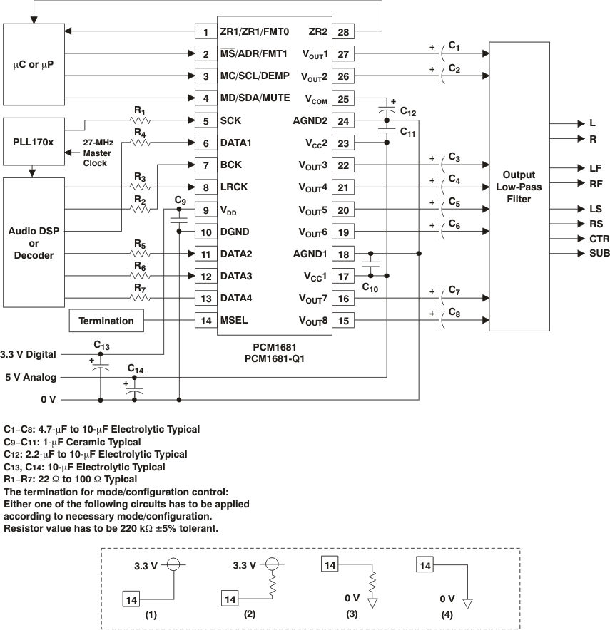
A basic connection diagram is shown in Figure 34, with the necessary power supply bypassing and decoupling components. Texas Instruments’ PLL170x is used to generate the system clock input at SCK, as well as generating the clock for the audio signal processor. The use of series resistors (22 Ω to 100 Ω) is recommended for SCK, LRCK, BCK, DATA1, DATA2, DATA3, and DATA4. The series resistor combines with the stray PCB capacitance and device input capacitance to form a low-pass filter that removes high-frequency noise from the digital signal, thus reducing high-frequency emission.
 Figure 34. Basic Connection Diagram
9.2.1 Design Requirements
- Control: Hardware, I2C, or SPI
- Audio Input: PCM Serial data, TDM, or DSP
- Audio Output: 3.75-Vpp analog audio
- Master Clock: PLL170X IC
9.2.2 Detailed Design Procedure
9.2.2.1 Hardware Control Method
There are 3 ways to control the PCM1681, hardware control, SPI, or I2C. Hardware control will provide a limited access to control features available in the PCM1681 but can be implemented with pull up and pull downs, or with GPIO of a microcontroller. Control via SPI or I2C will provide access to all control registers and features but will require a digital device that can implement SPI or I2C.
9.2.2.2 Audio Input
For audio input there are 3 options, PCM serial data, TDM, or DSP. All three will support the same quality of audio data, but having these 3 options to match the audio sources available outputs allows for greater flexibility. This selection is made by configuring the MSEL pin which is detailed in Table 7 and shown in Figure 34.
9.2.2.3 Audio Output
The output of the PCM1681 will produce a 3.75-Vpp signal at full scale into a 5-kΩ load, that should be filtered before being sent to an amplifier.
9.2.2.4 Master Clock
The master clock can come from wither a dedicated IC such as the PLL170X series, a crystal or the audio source IC. What is important is that the audio source and the PCM1681 are driven from the same source so that the audio clocks will be synchronous.
9.2.3 Application Curve
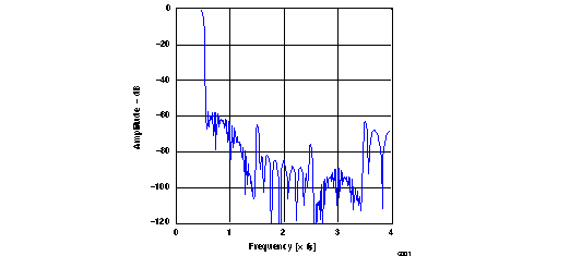
 Figure 35. Frequency Response (Sharp Roll-off)