SLES117B August 2004 – December 2015 PCM1794A
PRODUCTION DATA.
- 1 Features
- 2 Applications
- 3 Description
- 4 Revision History
- 5 Pin Configuration and Functions
- 6 Specifications
- 7 Detailed Description
- 8 Application and Implementation
- 9 Power Supply Recommendations
- 10Layout
- 11Device and Documentation Support
- 12Mechanical, Packaging, and Orderable Information
Package Options
Refer to the PDF data sheet for device specific package drawings
Mechanical Data (Package|Pins)
- DB|28
Thermal pad, mechanical data (Package|Pins)
Orderable Information
8 Application and Implementation
NOTE
Information in the following applications sections is not part of the TI component specification, and TI does not warrant its accuracy or completeness. TI’s customers are responsible for determining suitability of components for their purposes. Customers should validate and test their design implementation to confirm system functionality.
8.1 Application Information
The design of the application circuit lets the user realize the high signal-to-noise (S/N) ratio of the PCM1794A device, as noise and distortion generated in an application circuit are not negligible.
In the circuit of Figure 25, the output level is 2-VRMS, and 127-dB S/N is achieved. The circuit of Figure 26 should result in the highest performance. In this case the output level is set to 4.5-VRMS, and 129-dB S/N is achieved (stereo mode). In monaural mode, if the output of the L-channel and R-channel is used as a balanced output, 132-dB S/N is achieved (see Figure 27).
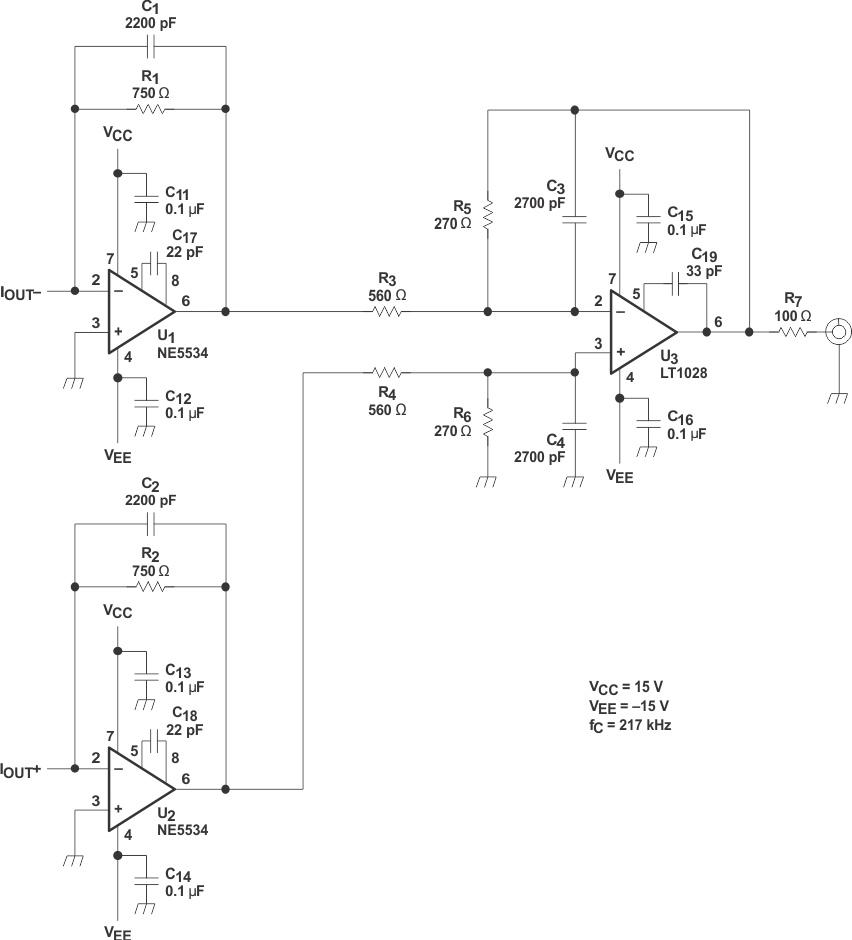 Figure 25. Measurement Circuit, VOUT = 2-VRMS
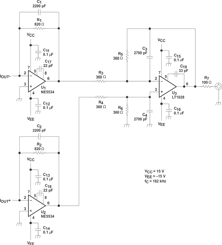 Figure 26. Measurement Circuit, VOUT = 4.5-VRMS
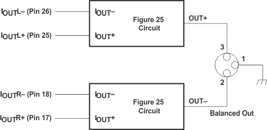 Figure 27. Measurement Circuit for Monaural Mode
8.1.1 I/V Section
The current of the PCM1794A device on each of the output pins (IOUTL+, IOUTL–, IOUTR+, IOUTR–) is 7.8 mA p-p at 0 dB (full scale). Use Equation 1 to calculate the voltage output level of the I/V converter (Vi).
where
- Rf is the feedback resistance of I/V converter
An NE5534 operational amplifier is recommended for the I/V circuit to obtain the specified performance. Dynamic performance such as the gain bandwidth, settling time, and slew rate of the operational amplifier affects the audio dynamic performance of the I/V section.
8.1.2 Differential Section
The PCM1794A voltage outputs are followed by differential amplifier stages, which sum the differential signals for each channel, creating a single-ended I/V op-amp output. In addition, the differential amplifiers provide a low-pass filter function.
The operational amplifier recommended for the differential circuit is the Linear Technology LT1028, because the input noise is low.
8.1.3 Interfacing With an External Digital Filter
For some applications, using a programmable digital signal processor as an external digital filter to perform the interpolation function may be necessary. The following pin settings enable the external digital filter application mode:
- MONO (pin 1) = LOW
- CHSL (pin 2) = HIGH
- FMT0 (pin 11) = HIGH
- FMT1 (pin 12) = HIGH
The pins that provide the serial interface for the external digital filter are shown in the connection diagram of Figure 28. The word clock (WDCK) must be operated at 8× or 4× the desired sampling frequency, fS.
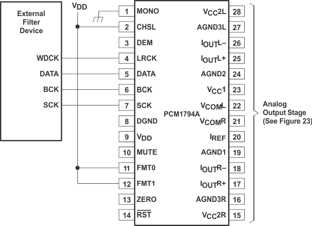 Figure 28. Connection Diagram for External Digital Filter (Internal DF Bypass Mode) Application
8.1.3.1 System Clock (SCK) and Interface Timing
In an application using an external digital filter, the PCM1794A device requires the synchronization of WDCK and the system clock. The system clock is phase-free with respect to WDCK. Interface timing among WDCK, BCK, and DATA is shown in Figure 29.
 Figure 29. Audio Interface Timing for External Digital Filter (Internal DF Bypass Mode) Application
Table 5 shows the timing requirements for an application using an external digital filter in internal DF bypass mode.
Table 5. External Digital Filter Application Timing Requirements
| MIN | MAX | UNIT | ||
|---|---|---|---|---|
| t(BCY) | BCK pulse-cycle time | 20 | ns | |
| t(BCL) | BCK pulse duration, LOW | 7 | ns | |
| t(BCH) | BCK pulse duration, HIGH | 7 | ns | |
| t(BL) | BCK rising edge to WDCK falling edge | 5 | ns | |
| t(LB) | WDCK falling edge to BCK rising edge | 5 | ns | |
| t(DS) | DATA setup time | 5 | ns | |
| t(DH) | DATA hold time | 5 | ns | |
8.1.3.2 Audio Format
The PCM1794A device in the external digital filter interface mode supports right-justified audio formats, including 24-bit audio data, as shown in Figure 30.
 Figure 30. Audio Data Input Format for External Digital Filter (Internal DF Bypass Mode) Application
8.2 Typical Application
This application is using the GPIO of a host controller to manipulate the hardware control pins. A PCM audio source is supplying digital audio and the output is single-ended stereo audio.
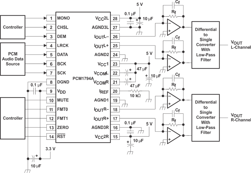 Figure 31. Typical Application Circuit
8.2.1 Design Requirements
For the typical application example, use the parameters listed in Table 6.
Table 6. Design Parameters
| DESIGN PARAMETER | EXAMPLE |
|---|---|
| Audio Input | Digital PCM |
| Audio Output | Single-Ended Stereo Analog |
| Control | Host GPIO |
| Filter | Internal Filter |
8.2.2 Detailed Design Procedure
8.2.2.1 Audio Input or Output
In this application, a PCM audio source is supplied to the device. A current output is produced and then converted to a voltage output in the I/V stage. The next stage in the output is a differential to single-ended amplifier stage with a low pass filter to reduce out of band noise. The fc of the example circuits (Figure 26 and Figure 27) are shown in the example figures. Use Equation 2 to calculate the value of fc.
8.2.3 Application Curves
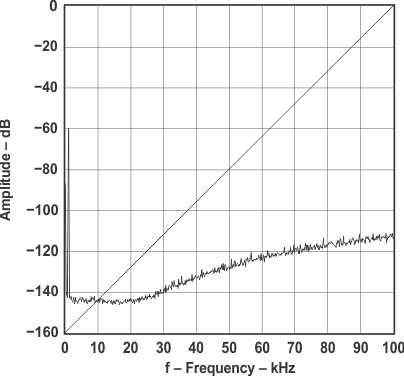
| VCC = 5 V | Measurement circuit is Figure 26 | |
| TA = 25°C | fS = 48 kHz, 32768 point 8 average | |
| VDD = 3.3 V | –60-db Output Spectrum, BW = 100 kHz | |
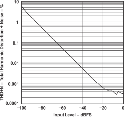
| VCC = 5 V | Measurement circuit is Figure 26 | |||
| VDD = 3.3 V | fS = 48 kHz, TA = 25°C | |||