SLES117B August 2004 – December 2015 PCM1794A
PRODUCTION DATA.
- 1 Features
- 2 Applications
- 3 Description
- 4 Revision History
- 5 Pin Configuration and Functions
- 6 Specifications
- 7 Detailed Description
- 8 Application and Implementation
- 9 Power Supply Recommendations
- 10Layout
- 11Device and Documentation Support
- 12Mechanical, Packaging, and Orderable Information
Package Options
Refer to the PDF data sheet for device specific package drawings
Mechanical Data (Package|Pins)
- DB|28
Thermal pad, mechanical data (Package|Pins)
Orderable Information
7 Detailed Description
7.1 Overview
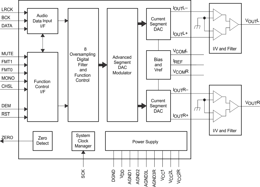
The PCM1794A device is a 24-bit, 192-kHz, differential-current, output digital-to-analog converter (DAC) that comes in a 28-pin SSOP package. The PCM1794AA device is hardware controlled and uses the advanced-segment DAC architecture from TI to perform with a Stereo Dynamic Range of 129 dB (132 dB Mono) and with a THD of 0.0004% at 44.1 kHz. The PCM1794AA device uses the SCK input as the system clock and automatically detects the sampling rate of the Digital Audio input when valid BCK and LRCK clocks are supplied. To bypass the internal filter, use an external digital filter.
Table 1. Device Features
| FEATURE | DESCRIPTION |
|---|---|
| Resolution | 24 bits |
| Audio data interface format | Standard, I2S, left justified |
| Audio data bit length | 16-bit, 24-bit selectable |
| Audio data format | MSB first, two's complement |
7.2 Functional Block Diagram

7.3 Feature Description
7.3.1 System Clock Input
The PCM1794A device requires a system clock for operating the digital interpolation filters and advanced segment DAC modulators. The system clock is applied at the SCK input (pin 7). The PCM1794A device has a system clock detection circuit that automatically senses the frequency at which the system clock is operating. Table 2 shows examples of system clock frequencies for common audio-sampling rates.
The Timing Requirements table lists and Figure 1 shows the timing requirements for the system clock input. For optimal performance, use a clock source with low-phase jitter and noise. One of the Texas Instruments PLL1700 family of multiclock generators is an excellent selection for providing the PCM1794A system clock.
Table 2. System Clock Rates for Common Audio Sampling Frequencies
| SAMPLING FREQUENCY | SYSTEM CLOCK FREQUENCY (fSCK) (MHz) | |||||
|---|---|---|---|---|---|---|
| 128 fS | 192 fS | 256 fS | 384 fS | 512 fS | 768 fS | |
| 32 kHz | 4.096 | 6.144 | 8.192 | 12.288 | 16.384 | 24.576 |
| 44.1 kHz | 5.6488 | 8.4672 | 11.2896 | 16.9344 | 22.5792 | 33.8688 |
| 48 kHz | 6.144 | 9.216 | 12.288 | 18.432 | 24.576 | 36.864 |
| 96 kHz | 12.288 | 18.432 | 24.576 | 36.864 | 49.152 | 73.728 |
| 192 kHz | 24.576 | 36.864 | 49.152 | 73.728 | See (1) | See (1) |
7.3.2 Power-On and External Reset Functions
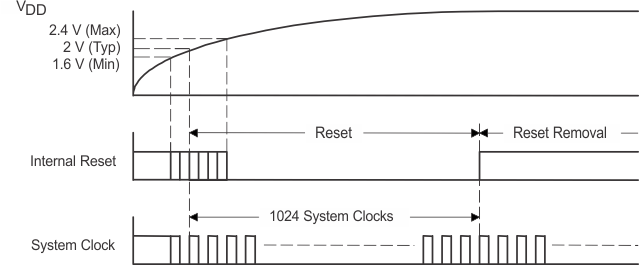
The PCM1794A device includes a power-on reset function. Figure 21 shows the operation of this function. With VDD > 2 V, the power-on reset function is enabled. The initialization sequence requires 1024 system clocks from the time VDD > 2 V.
The PCM1794A device also includes an external reset capability using the RST input (pin 14), which allows an external controller or master reset circuit to force the PCM1794A device to initialize to its default reset state.
The Timing Requirements table lists and Figure 2 shows the external reset operation and timing. The RST pin is set to logic 0 for a minimum of 20 ns. The RST pin is then set to a logic 1 state to start the initialization sequence, which requires 1024 system clock periods. The external reset is useful in applications with a delay between the PCM1794A power-up and system clock activation.
 Figure 21. Power-On Reset Timing
7.3.3 Audio Data Interface
7.3.3.1 Audio Serial Interface
The audio interface port is a 3-wire serial port that includes LRCK (pin 4), BCK (pin 6), and DATA (pin 5). BCK is the serial audio bit clock, and used to clock the serial data present on DATA into the serial shift register of the audio interface. Serial data is clocked into the PCM1794A device on the rising edge of BCK. LRCK is the serial audio left/right word clock.
The PCM1794A device requires the synchronization of LRCK and the system clock, but does not require a specific phase relation between LRCK and the system clock.
If the relationship between LRCK and the system clock changes more than ±6 BCK, internal operation is initialized within 1/fS, and the analog outputs are forced to the bipolar zero level until resynchronization between LRCK and the system clock is completed.
7.3.3.2 PCM Audio Data Formats and Timing
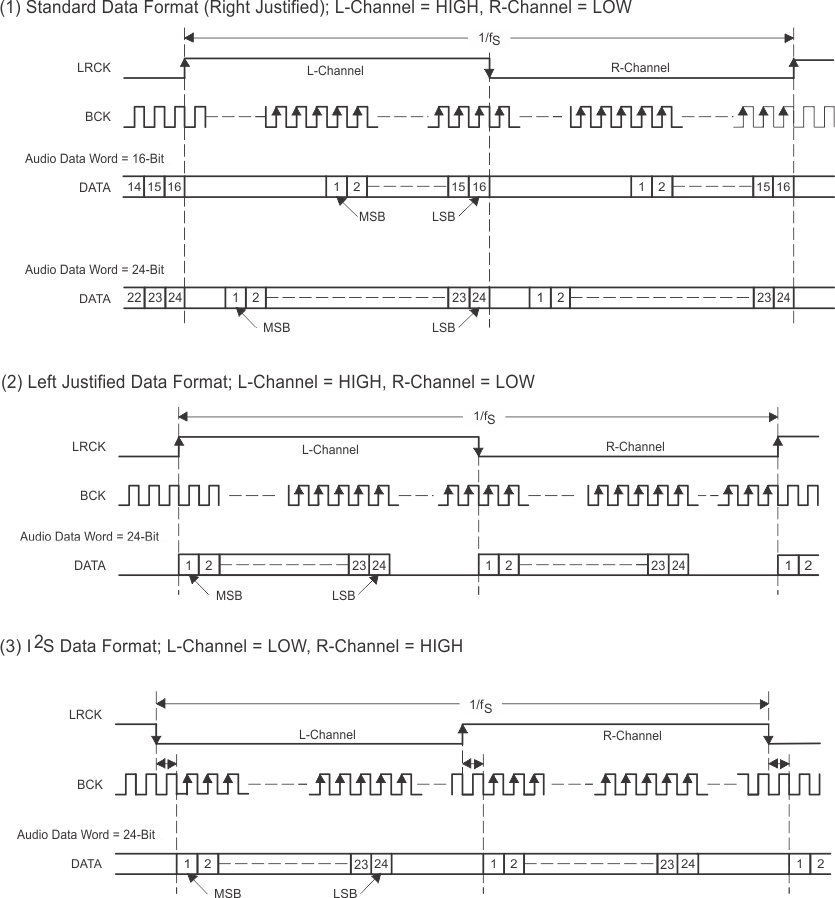
The PCM1794A device supports industry-standard audio data formats, including standard right-justified, I2S, and left-justified. The data formats are shown in Figure 22. Data formats are selected using the format bits, FMT1 (pin 12), and FMT0 (pin 11) as shown in Table 3. All formats require binary twos-complement, MSB-first audio data. The Timing Requirements table lists and Figure 3 shows a detailed timing diagram for the serial audio interface.
 Figure 22. Audio Data Input Formats
7.3.4 Audio Data Format
Audio format is selected using FMT0 (pin 11) and FMT1 (pin 12). The PCM1794A device also supports monaural mode and DF bypass mode using MONO (pin 1) and CHSL (pin 2). The PCM1794A device can select the DF rolloff characteristics.
Table 3. Audio Data Format Select
| MONO | CHSL | FMT1 | GMT0 | FORMAT | STEREO/MONO | DF ROLLOFF |
|---|---|---|---|---|---|---|
| 0 | 0 | 0 | 0 | I2S | Stereo | Sharp |
| 0 | 0 | 0 | 1 | Left-justified format | Stereo | Sharp |
| 0 | 0 | 1 | 0 | Standard, 16-bit | Stereo | Sharp |
| 0 | 0 | 1 | 1 | Standard, 24-bit | Stereo | Sharp |
| 0 | 1 | 0 | 0 | I2S | Stereo | Slow |
| 0 | 1 | 0 | 1 | Left-justified format | Stereo | Slow |
| 0 | 1 | 1 | 0 | Standard, 16-bit | Stereo | Slow |
| 0 | 1 | 1 | 1 | Digital filter bypass | Mono | — |
| 1 | 0 | 0 | 0 | I2S | Mono, L-channel | Sharp |
| 1 | 0 | 0 | 1 | Left-justified format | Mono, L-channel | Sharp |
| 1 | 0 | 1 | 0 | Standard, 16-bit | Mono, L-channel | Sharp |
| 1 | 0 | 1 | 1 | Standard, 24-bit | Mono, L-channel | Sharp |
| 1 | 1 | 0 | 0 | I2S | Mono, R-channel | Sharp |
| 1 | 1 | 0 | 1 | Left-justified format | Mono, R-channel | Sharp |
| 1 | 1 | 1 | 0 | Standard, 16-bit | Mono, R-channel | Sharp |
| 1 | 1 | 1 | 1 | Standard, 24-bit | Mono, R-channel | Sharp |
7.3.5 Soft Mute
The PCM1794A device supports mute operation. When MUTE (pin 10) is set to HIGH, both analog outputs transition to the bipolar zero level in –0.5-dB steps with a transition speed of 1/fS per step. The mute operation system provides pop-free muting of the DAC output.
7.3.6 De-Emphasis
The PCM1794A device has a de-emphasis filter for the sampling frequency of 44.1 kHz. The de-emphasis filter is controlled using DEM (pin 3).
7.3.7 Zero Detect
When the PCM1794A device detects that the audio input data in the L-channel and the R-channel is continuously zero for 1024 LRCKs in the PCM mode, or that the audio input data is continuously zero for 1024 WDCKs in the external filter mode, the PCM1794A device sets ZERO (pin 13) to HIGH.
7.3.8 Advanced Segment DAC
 Figure 23. Advanced Segment DAC
The PCM1794A device uses TI’s advanced segment DAC architecture to achieve excellent dynamic performance and improved tolerance to clock jitter. The PCM1794A device provides balanced current outputs.
Digital input data using the digital filter is separated into 6 upper bits and 18 lower bits. The 6 upper bits are converted to inverted complementary offset binary (ICOB) code. The lower 18 bits, associated with the MSB, are processed by a five-level, third-order delta-sigma modulator operated at 64 fS by default. The 1 level of the modulator is equivalent to the 1 LSB of the ICOB code converter. The data groups processed in the ICOB converter and third-order delta-sigma modulator are summed together to create an up-to-66-level digital code, and then processed by data-weighted averaging (DWA) to reduce the noise produced by element mismatch. The data of up to 66 levels from the DWA is converted to an analog output in the differential-current segment section.
This architecture has overcome the various drawbacks of conventional multibit processing, and also achieves excellent dynamic performance.
7.3.9 Analog Output
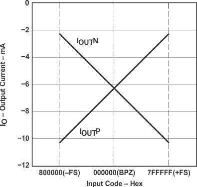
Table 4 and Figure 24 show the relationship between the digital input code and analog output.
Table 4. Digital Input Code and Analog Output
| 800000 (–FS) | 000000 (BPZ) | 7FFFFF (+FS) | |
|---|---|---|---|
| IOUTN [mA] | –2.3 | –6.2 | –10.1 |
| IOUTP [mA] | –10.1 | –6.2 | –2.3 |
| VOUTN [V](1) | –1.725 | –4.65 | –7.575 |
| VOUTP [V](1) | –7.575 | –4.65 | –1.725 |
| VOUT [V](1) | –2.821 | 0 | 2.821 |
 Figure 24. Relationship Between Digital Input and Analog Output
7.4 Device Functional Modes
7.4.1 Device Control
The PCM1794A device is a hardware controlled by external pins. These pins can be tied high or low directly to GND or to VDD. These pins can also be controlled by the GPIO of a host controller.
7.4.2 Audio Input Modes
The PCM1794A device accepts PCM audio in I2S, Right justified (standard), or Left justified formats. The PCM1794 device has an internal digital filter that has the option of a slow or sharp roll off. Use an external digital filter to bypass the internal digital filter. External filter mode is explained more in the Interfacing With an External Digital Filter section.