SBOS207C October 2001 – December 2015 PGA2310
PRODUCTION DATA.
- 1 Features
- 2 Applications
- 3 Description
- 4 Revision History
- 5 Pin Configuration and Functions
- 6 Specifications
- 7 Detailed Description
- 8 Application and Implementation
- 9 Power Supply Recommendations
- 10Layout
- 11Device and Documentation Support
- 12Mechanical, Packaging, and Orderable Information
Package Options
Mechanical Data (Package|Pins)
Thermal pad, mechanical data (Package|Pins)
- DW|16
Orderable Information
8 Application and Implementation
NOTE
Information in the following applications sections is not part of the TI component specification, and TI does not warrant its accuracy or completeness. TI’s customers are responsible for determining suitability of components for their purposes. Customers should validate and test their design implementation to confirm system functionality.
8.1 Application Information
The PGA2310 is commonly used as a digitally controlled analog volume control. Analog volume is controlled through a serial interface in 0.5-dB steps, ranging from a gain of 31.5 dB down to an attenuation of −95.5 dB.
8.2 Typical Application
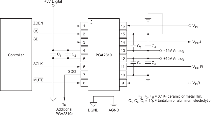
Figure 13 depicts the recommended connections for the PGA2310.
 Figure 13. Recommended Connection Diagram
8.2.1 Design Requirements
- Wide dynamic range: 35.5 dB to –95.5 dB
- Operate from 5-V digital supply and ±15-V analog supplies
- Digitally controlled analog volume
8.2.2 Detailed Design Procedure
The PGA2310 is a complete digitally controlled analog stereo volume controller system on a chip requiring only a controller to select the gain or attenuation through a serial interface. Figure 13 illustrates the basic connections to the PGA2310. Power-supply bypass capacitors should be placed as close to the PGA2310 package as physically possible.
8.2.3 Application Curve
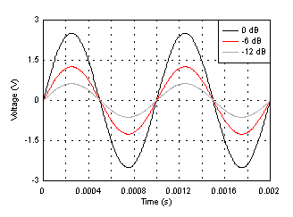
 Figure 14. PGA2310 Operating at 0 dB, –6 dB and –12 dB