SBVS299A April 2017 – September 2025 REF31-Q1
PRODUCTION DATA
- 1
- 1 Features
- 2 Applications
- 3 Description
- 4 Device Comparison Table
- 5 Pin Configuration and Functions
- 6 Specifications
- 7 Detailed Description
- 8 Application and Implementation
- 9 Device and Documentation Support
- 10Revision History
- 11Mechanical, Packaging, and Orderable Information
Package Options
Mechanical Data (Package|Pins)
- DBZ|3
Thermal pad, mechanical data (Package|Pins)
Orderable Information
7.3.1 Supply Voltage
The REF31xx-Q1 family of references features an extremely low dropout voltage. With the exception of the REF3112, which has a minimum supply requirement of 1.8 V, these references can be operated with a supply of only 5 mV above the output voltage in an unloaded condition. For loaded conditions, a typical dropout voltage versus load is shown in Typical Characteristics.
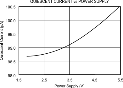
The REF31xx-Q1 features a low quiescent current that is extremely stable over changes in both temperature and supply. The typical room temperature quiescent current is 100 μA, and the maximum quiescent current over temperature is just 135 μA. The quiescent current typically changes less than 2 μA over the entire supply range, as shown in Figure 7-1.
 Figure 7-1 Supply Current vs Supply Voltage
Supply voltages below the specified levels can cause the REF31xx-Q1 to momentarily draw currents greater than the typical quiescent current. This can be prevented by using a power supply with a fast rising edge and low output impedance.