SBVS299A April 2017 – September 2025 REF31-Q1
PRODUCTION DATA
- 1
- 1 Features
- 2 Applications
- 3 Description
- 4 Device Comparison Table
- 5 Pin Configuration and Functions
- 6 Specifications
- 7 Detailed Description
- 8 Application and Implementation
- 9 Device and Documentation Support
- 10Revision History
- 11Mechanical, Packaging, and Orderable Information
Package Options
Mechanical Data (Package|Pins)
- DBZ|3
Thermal pad, mechanical data (Package|Pins)
Orderable Information
8.2 Typical Application
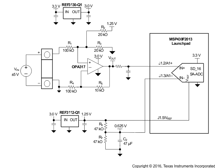
Figure 8-2 shows a low-power reference and conditioning circuit. This circuit attenuates and level-shifts a bipolar input voltage within the proper input range of a single-supply, low-power, 16-bit ΔΣ ADC, such as the one inside the MSP430™ or other similar single-supply ADCs. Precision reference circuits are used to level-shift the input signal, provide the ADC reference voltage, and to create a well-regulated supply voltage for the low-power analog circuitry. A low-power, zero-drift, op-amp circuit is used to attenuate and level-shift the input signal.
 Figure 8-2 Low-Power Reference and Bipolar Voltage
Conditioning Circuit for Low-Power ADCs