SBVS046D December 2003 – March 2016 REF3112 , REF3120 , REF3125 , REF3130 , REF3133 , REF3140
PRODUCTION DATA.
- 1 Features
- 2 Applications
- 3 Description
- 4 Revision History
- 5 Device Comparison Table
- 6 Pin Configuration and Functions
- 7 Specifications
- 8 Detailed Description
- 9 Application and Implementation
- 10Power Supply Recommendations
- 11Layout
- 12Device and Documentation Support
- 13Mechanical, Packaging, and Orderable Information
Package Options
Refer to the PDF data sheet for device specific package drawings
Mechanical Data (Package|Pins)
- DBZ|3
Thermal pad, mechanical data (Package|Pins)
Orderable Information
7 Specifications
7.1 Absolute Maximum Ratings
over operating free-air temperature range (unless otherwise noted)(1)| MIN | MAX | UNIT | ||
|---|---|---|---|---|
| Supply voltage, V+ to V– | 7 | V | ||
| Output short circuit | Continuous | |||
| Operating temperature | –55 | 135 | °C | |
| Junction temperature | 150 | °C | ||
| Storage temperature, Tstg | –65 | 150 | °C | |
(1) Stresses beyond those listed under Absolute Maximum Ratings may cause permanent damage to the device. These are stress ratings only, which do not imply functional operation of the device at these or any other conditions beyond those indicated under Recommended Operating Conditions. Exposure to absolute-maximum-rated conditions for extended periods may affect device reliability.
7.2 ESD Ratings
| VALUE | UNIT | |||
|---|---|---|---|---|
| V(ESD) | Electrostatic discharge | Human-body model (HBM), per ANSI/ESDA/JEDEC JS-001(1) | ±2000 | V |
| Charged-device model (CDM), per JEDEC specification JESD22-C101(2) | ±1000 | |||
(1) JEDEC document JEP155 states that 500-V HBM allows safe manufacturing with a standard ESD control process.
(2) JEDEC document JEP157 states that 250-V CDM allows safe manufacturing with a standard ESD control process.
7.3 Recommended Operating Conditions
over operating free-air temperature range (unless otherwise noted)| MIN | MAX | UNIT | ||
|---|---|---|---|---|
| VIN | Input voltage | VREF + 0.05(1) | 5.5 | V |
| ILOAD | Load current | 25 | mA | |
| TA | Operating temperature | –40 | 125 | °C |
(1) Minimum supply voltage for the REF3112 is 1.8 V.
7.4 Thermal Information
| THERMAL METRIC(1) | REF31xx | UNIT | |
|---|---|---|---|
| DBZ (SOT-23) | |||
| 3 PINS | |||
| RθJA | Junction-to-ambient thermal resistance | 292.9 | °C/W |
| RθJC(top) | Junction-to-case (top) thermal resistance | 124.4 | °C/W |
| RθJB | Junction-to-board thermal resistance | 89 | °C/W |
| ψJT | Junction-to-top characterization parameter | 11.4 | °C/W |
| ψJB | Junction-to-board characterization parameter | 87.6 | °C/W |
| RθJC(bot) | Junction-to-case (bottom) thermal resistance | — | °C/W |
(1) For more information about traditional and new thermal metrics, see the Semiconductor and IC Package Thermal Metrics application report, SPRA953.
7.5 Electrical Characteristics
at TA = 25°C, ILOAD = 0 mA, and VIN = 5 V (unless otherwise noted)| PARAMETER | TEST CONDITIONS | MIN | TYP | MAX | UNIT | |||
|---|---|---|---|---|---|---|---|---|
| REF3312(1) — 1.25 V | ||||||||
| VOUT | Output voltage | 1.2475 | 1.25 | 1.2525 | V | |||
| Initial accuracy | –0.2% | 0.2% | ||||||
| Output voltage noise | f = 0.1 Hz to 10 Hz | 17 | μVPP | |||||
| f = 10 Hz to 10 kHz | 24 | μVRMS | ||||||
| REF3120 — 2.048 V | ||||||||
| VOUT | Output voltage | 2.0439 | 2.048 | 2.0521 | V | |||
| Initial accuracy | –0.2% | 0.2% | ||||||
| Output voltage noise | f = 0.1Hz to 10Hz | 27 | μVPP | |||||
| f = 10Hz to 10kHz | 39 | μVRMS | ||||||
| REF3125 — 2.5 V | ||||||||
| VOUT | Output voltage | 2.495 | 2.5 | 2.505 | V | |||
| Initial accuracy | –0.2% | 0.2% | ||||||
| Output voltage noise | f = 0.1Hz to 10Hz | 33 | μVPP | |||||
| f = 10Hz to 10kHz | 48 | μVRMS | ||||||
| REF3130 — 3 V | ||||||||
| VOUT | Output voltage | 2.994 | 3 | 3.006 | V | |||
| Initial accuracy | –0.2% | 0.2% | ||||||
| Output voltage noise | f = 0.1Hz to 10Hz | 39 | μVPP | |||||
| f = 10Hz to 10kHz | 57 | μVRMS | ||||||
| REF3133 — 3.3 V | ||||||||
| VOUT | Output voltage | 3.2934 | 3.3 | 3.3066 | V | |||
| Initial accuracy | –0.2% | 0.2% | ||||||
| Output voltage noise | f = 0.1Hz to 10Hz | 43 | μVPP | |||||
| f = 10Hz to 10kHz | 63 | μVRMS | ||||||
| REF3140 — 4.096 V | ||||||||
| VOUT | Output voltage | 4.0878 | 4.096 | 4.1042 | V | |||
| Initial accuracy | –0.2% | 0.2% | ||||||
| Output voltage noise | f = 0.1Hz to 10Hz | 53 | μVPP | |||||
| f = 10Hz to 10kHz | 78 | μVRMS | ||||||
| REF31xx (REF3112, REF3120, REF3125, REF3130, REF3133, REF3140) | ||||||||
| dVOUT/dT | Output voltage temperature drift(2) | TA = 0°C to 70°C. | 5 | 15 | ppm/°C | |||
| TA = –40°C to +125°C . | 10 | 20 | ||||||
| Long-term stability | 0 to 1000 hours | 70 | ppm | |||||
| Line regulation | VREF + 0.05(1) ≤ VIN ≤ 5.5V | 20 | 65 | ppm/V | ||||
| dVOUT/dILOAD | Load regulation(3) | Sourcing | 0mA < ILOAD < 10mA, VIN = VREF + 250mV(1) | 10 | 30 | µV/mA | ||
| Sinking | –10mA < ILOAD < 0mA, VIN = VREF + 100mV(1) | 20 | 50 | |||||
| dT | Thermal hysteresis(4) | First Cycle | 100 | ppm | ||||
| Additional Cycles | 25 | |||||||
| VIN – VOUT | Dropout voltage(1) | TA = –40°C to +125°C. | 5 | 50 | mV | |||
| ILOAD | Output current | –10 | 10 | mA | ||||
| ISC | Short-circuit current | Sourcing | 50 | mA | ||||
| Sinking | 40 | |||||||
| Turnon settling time | To 0.1% at VIN = +5V with CL = 0μF | 400 | µs | |||||
| POWER SUPPLY | ||||||||
| VS | Voltage | ILOAD = 0, TA = –40°C to +125°C. | VREF + 0.05(1) | 5.5 | V | |||
| IQ | Quiescent current | ILOAD = 0, TA = 25°C | 100 | 115 | µA | |||
| ILOAD = 0, TA = –40°C to +125°C | 115 | 135 | ||||||
(1) Minimum supply voltage for the REF3112 is 1.8 V.
(2) Box Method used to determine temperature drift.
(3) Typical value of load regulation reflects measurements using force and sense contacts; see Load Regulation.
(4) Thermal hysteresis is explained in more detail in Application and Implementation of this data sheet.
7.6 Typical Characteristics
At TA = 25°C, VIN = 5-V power supply, and REF3125 is used for typical characteristic measurements, unless otherwise noted.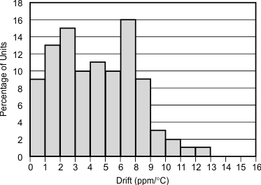 Figure 1. Temperature Drift (0°C to 70°C)
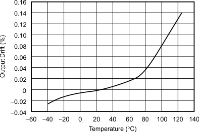 Figure 3. Output Voltage vs Temperature
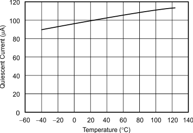 Figure 5. Quiescent Current vs Temperature
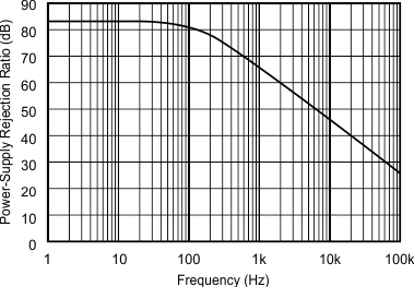 Figure 7. PSRR vs Frequency
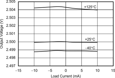 Figure 9. Output Voltage vs Load Current
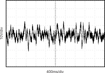 Figure 11. 0.1-Hz to 10-Hz Noise
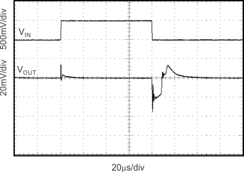 Figure 13. Line Transient CL = 0 pF
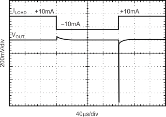 Figure 15. Load Transient CL = 0 pF, ±10-mA Output Pulse
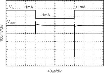 Figure 17. Load Transient CL = 0 pF, ±1-mA Output Pulse
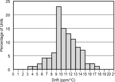 Figure 2. Temperature Drift (–40°C to +125°C)
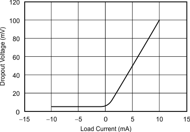 Figure 4. Dropout Voltage vs Load Current
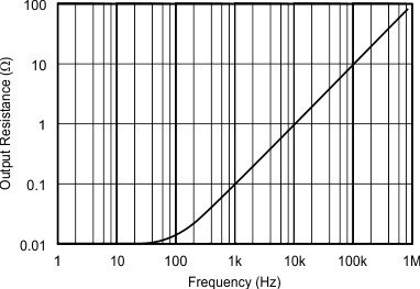 Figure 6. Output Impedance vs Frequency
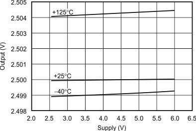 Figure 8. Output vs Supply
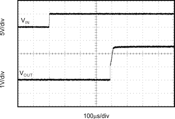 Figure 10. Step Response, CL = 0, 5-V Start-Up
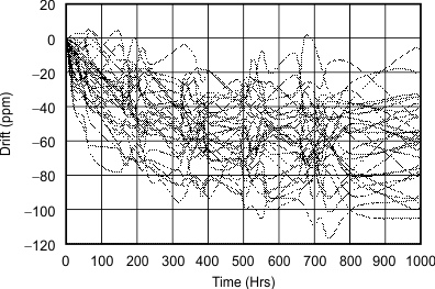 Figure 12. REF3112 Long-Term Stability
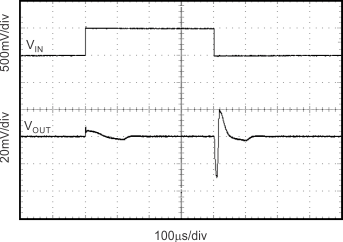 Figure 14. Line Transient CL = 10 μF
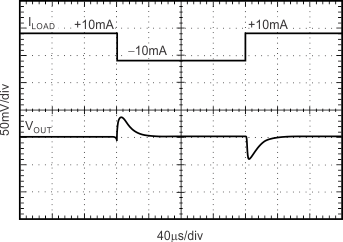 Figure 16. Load Transient CL = 1 µF, ±10-mA Output Pulse
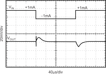 Figure 18. Load Transient CL = 1 µF, ±1-mA Output Pulse
