SNAS795A February   2020  – July 2020 REF4132-Q1

PRODUCTION DATA.  

  1. Features
  2. Applications
  3. Description
    1.     Device Images
      1.      Simplified Schematic
      2.      Dropout vs. Current Load Over Temperature
  4. Revision History
  5. Device Comparison Table
  6. Pin Configuration and Functions
    1.     Pin Functions
  7. Specifications
    1. 7.1      Absolute Maximum Ratings
    2. 7.2      ESD Ratings
    3. 7.3      Recommended Operating Conditions
    4. 7.4      Thermal Information
    5. Table 1. Electrical Characteristics
    6. 7.5      Typical Characteristics
  8. Parameter Measurement Information
    1. 8.1 Solder Heat Shift
    2. 8.2 Long-Term Stability
    3. 8.3 Thermal Hysteresis
    4. 8.4 Power Dissipation
    5. 8.5 Noise Performance
  9. Detailed Description
    1. 9.1 Overview
    2. 9.2 Functional Block Diagram
    3. 9.3 Feature Description
      1. 9.3.1 Supply Voltage
      2. 9.3.2 Low Temperature Drift
      3. 9.3.3 Load Current
    4. 9.4 Device Functional Modes
      1. 9.4.1 EN Pin
      2. 9.4.2 Negative Reference Voltage
  10. 10Application and Implementation
    1. 10.1 Application Information
    2. 10.2 Typical Application: Basic Voltage Reference Connection
      1. 10.2.1 Design Requirements
      2. 10.2.2 Detailed Design Procedure
        1. 10.2.2.1 Input and Output Capacitors
        2. 10.2.2.2 VIN Slew Rate Considerations
        3. 10.2.2.3 Shutdown/Enable Feature
      3. 10.2.3 Application Curves
  11. 11Power Supply Recommendations
  12. 12Layout
    1. 12.1 Layout Guidelines
    2. 12.2 Layout Example
  13. 13Device and Documentation Support
    1. 13.1 Documentation Support
      1. 13.1.1 Related Documentation
    2. 13.2 Receiving Notification of Documentation Updates
    3. 13.3 Support Resources
    4. 13.4 Trademarks
    5. 13.5 Electrostatic Discharge Caution
    6. 13.6 Glossary
  14. 14Mechanical, Packaging, and Orderable Information

Package Options

Mechanical Data (Package|Pins)
Thermal pad, mechanical data (Package|Pins)
Orderable Information

Supply Voltage

The REF4132-Q1 voltage reference features an extremely low dropout voltage. For loaded conditions, a typical dropout voltage versus load is shown on the front page. The REF4132-Q1 features a low quiescent current that is extremely stable over changes in both temperature and supply. The typical room temperature quiescent current is 75 μA, and the maximum quiescent current over temperature is just 100 μA. Supply voltages below the specified levels can cause the REF4132-Q1 to momentarily draw currents greater than the typical quiescent current. Use a power supply with a fast rising edge and low output impedance to easily prevent this issue.

The supply current vs supply voltage figure is shown in Figure 26.
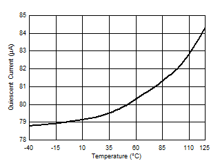
REF4132-Q1 D003_VinvsIq.gifFigure 26. Supply Current vs Supply Voltage