SBOS471B April 2010 – June 2015 REF5020-EP , REF5025-EP , REF5040-EP , REF5050-EP
PRODUCTION DATA.
- 1 Features
- 2 Applications
- 3 Description
- 4 Revision History
- 5 Pin Configuration and Functions
- 6 Specifications
- 7 Detailed Description
- 8 Application and Implementation
- 9 Power Supply Recommendations
- 10Layout
- 11Device and Documentation Support
- 12Mechanical, Packaging, and Orderable Information
Package Options
Mechanical Data (Package|Pins)
- D|8
Thermal pad, mechanical data (Package|Pins)
Orderable Information
7 Detailed Description
7.1 Overview
The REF50xx devices are low-noise, low-drift, very high precision voltage references. These references can both sink and source, and are very robust with regard to line and load changes.
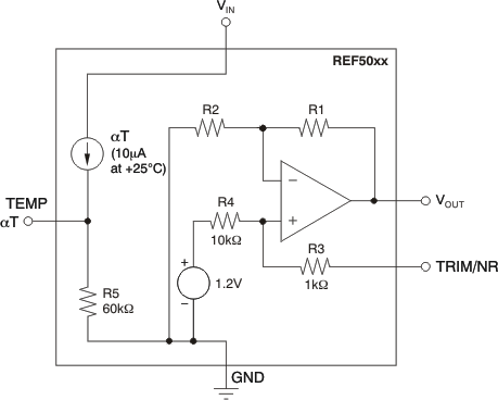
7.2 Functional Block Diagram

7.3 Feature Description
7.3.1 Output Adjustment Using The TRIM/NR Pin
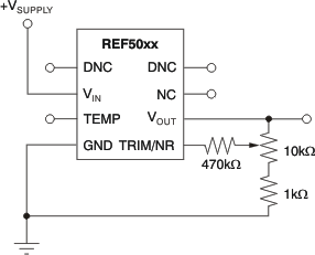
The REF50xx provides a very accurate, factory-trimmed voltage output. However, VOUT can be adjusted using the trim and noise reduction pin (TRIM/NR, pin 5). Figure 22 shows a typical circuit that allows an output adjustment of ±15 mV
 Figure 22. VOUT Adjustment Using the TRIM/NR Pin
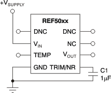
The REF50xx allows access to the bandgap through the TRIM/NR pin. Placing a capacitor from the TRIM/NR pin to GND (see Figure 24) in combination with the internal R3 and R4 resistors creates a low-pass filter. A capacitance of 1 μF creates a low-pass filter with the corner frequency between 10 Hz and 20 Hz. Such a filter decreases the overall noise measured on the VOUT pin by half. Higher capacitance results in a lower filter cutoff frequency, further reducing output noise. Use of this capacitor increases start-up time.
7.3.2 Low Temperature Drift
The REF50xx is designed for minimal drift error, which is defined as the change in output voltage over temperature. The drift is calculated using the box method, as described by Equation 1:

The REF50xx features a maximum drift coefficient of 3 ppm/°C for the high-grade version, and 8 ppm/°C for the standard-grade.
7.3.3 Temperature Monitoring
The temperature output terminal (TEMP, pin 3) provides a temperature-dependent voltage output with approximately 60-kΩ source impedance. As seen in Figure 8, the output voltage follows the nominal relationship:
This pin indicates general chip temperature, accurate to approximately ±15°C. Although it is not generally suitable for accurate temperature measurements, it can be used to indicate temperature changes or for temperature compensation of analog circuitry. A temperature change of 30°C corresponds to an approximate 79 mV change in voltage at the TEMP pin.
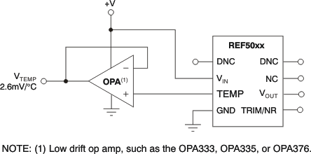
The TEMP pin has high output impedance (see Functional Block Diagram). Loading this pin with a low-impedance circuit induces a measurement error; however, it does not have any effect on VOUT accuracy. To avoid errors caused by low-impedance loading, buffer the TEMP pin output with a suitable low-temperature drift operational amplifiers, such as the OPA333, OPA335, or OPA376, as shown in Figure 23.
 Figure 23. Buffering the TEMP Pin Output
7.3.4 Noise Performance
Typical 0.1-Hz to 10-Hz voltage noise for each member of the REF50xx family is specified in the Electrical Characteristics: Per Device table. The noise voltage increases with output voltage and operating temperature. Additional filtering can be used to improve output noise levels, although take care to ensure the output impedance does not degrade performance.
For additional information about how to minimize noise and maximize performance in mixed-signal applications such as data converters, refer to the series of Analog Applications Journal articles entitled, How a Voltage Reference Affects ADC Performance. This three-part series is available for download from the TI website under three literature numbers: SLYT331, SLYT339, and SLYT355, respectively.
 Figure 24. Noise Reduction Using the TRIM/NR Pin
7.4 Device Functional Modes
The REF50xx is powered on when the voltage on the VIN pin is greater than VOUT + 0.2 V, except for the REF5020 and REF5025, where the minimum supply voltage is 2.7 V. The maximum input voltage for the REF50xx is 18 V. Use a supply bypass capacitor ranging from 1 μF to 10 μF. The total capacitive load at the output must be between 1 μF to 50 μF to ensure best output stability.