SBOS708B May   2016  – August 2016 REF6025 , REF6030 , REF6033 , REF6041 , REF6045 , REF6050

PRODUCTION DATA.  

  1. Features
  2. Applications
  3. Description
    1.     Device Images
      1.      Typical Application
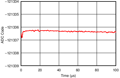
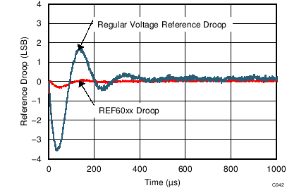
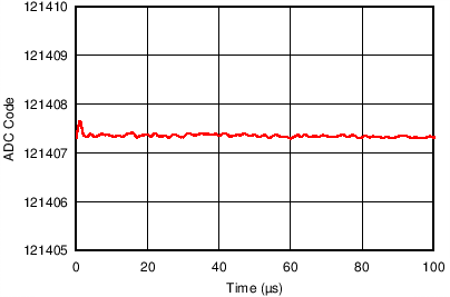
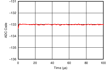
      2.      Reference Droop comparison (1 LSB = 19.07 µV, With ADS8881 at 1 MSPS)
  4. Revision History
  5. Device Comparison Table
  6. Pin Configuration and Functions
    1.     Pin Functions
  7. Specifications
    1. 7.1 Absolute Maximum Ratings
    2. 7.2 ESD Ratings
    3. 7.3 Recommended Operating Conditions
    4. 7.4 Thermal Information
    5. 7.5 Electrical Characteristics
    6. 7.6 Typical Characteristics
  8. Parameter Measurement Information
    1. 8.1 Solder Heat Shift
    2. 8.2 Thermal Hysteresis
    3. 8.3 Reference Droop Measurements
    4. 8.4 1/f Noise Performance
  9. Detailed Description
    1. 9.1 Overview
    2. 9.2 Functional Block Diagram
    3. 9.3 Feature Description
      1. 9.3.1 Integrated ADC Drive Buffer
      2. 9.3.2 Temperature Drift
      3. 9.3.3 Load Current
      4. 9.3.4 Stability
    4. 9.4 Device Functional Modes
  10. 10Applications and Implementation
    1. 10.1 Application Information
    2. 10.2 Typical Application
      1. 10.2.1 Design Requirements
      2. 10.2.2 Detailed Design Procedure
        1. 10.2.2.1 Results
      3. 10.2.3 Application Curves
  11. 11Power Supply Recommendations
  12. 12Layout
    1. 12.1 Layout Guidelines
    2. 12.2 Layout Example
  13. 13Device and Documentation Support
    1. 13.1 Documentation Support
      1. 13.1.1 Related Documentation
    2. 13.2 Related Links
    3. 13.3 Receiving Notification of Documentation Updates
    4. 13.4 Community Resources
    5. 13.5 Trademarks
    6. 13.6 Electrostatic Discharge Caution
    7. 13.7 Glossary
  14. 14Mechanical, Packaging, and Orderable Information

Package Options

Mechanical Data (Package|Pins)
Thermal pad, mechanical data (Package|Pins)
Orderable Information

Typical Characteristics

at TA = 25°C, IL = 0 mA, and VIN = 5 V, using REF6025 (unless otherwise noted)
REF6025 REF6030 REF6033 REF6041 REF6045 REF6050 C002_SBOS708.png
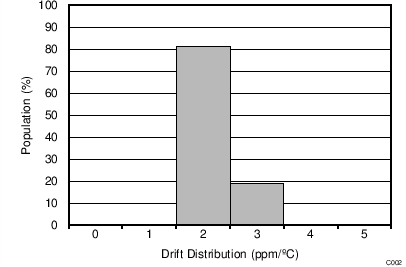
TA = –40°C to +125°C
Figure 1. Drift Distribution
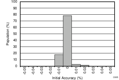
REF6025 REF6030 REF6033 REF6041 REF6045 REF6050 C005_SBOS708.png
Figure 3. Initial Accuracy Distribution
REF6025 REF6030 REF6033 REF6041 REF6045 REF6050 C001_SBOS708.png
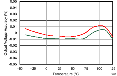
Figure 5. Output Voltage Accuracy vs Temperature
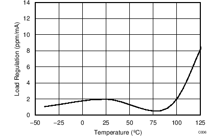
REF6025 REF6030 REF6033 REF6041 REF6045 REF6050 C006_SBOS708.png
VIN = VOUT + 600 mV,
IL = 0 mA to 4 mA
Figure 7. Load Regulation Sourcing vs Temperature
REF6025 REF6030 REF6033 REF6041 REF6045 REF6050 C010_SBOS748.png
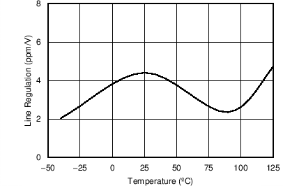
VOUT + 0.25 V ≤ VIN ≤ 5.5 V
Figure 9. Line Regulation vs Temperature
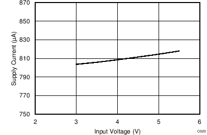
REF6025 REF6030 REF6033 REF6041 REF6045 REF6050 C020_SBOS708.png
Figure 11. Supply Current vs Input Voltage
REF6025 REF6030 REF6033 REF6041 REF6045 REF6050 C021_SBOS708.png
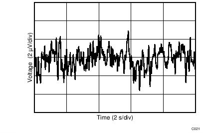
Figure 13. 0.1-Hz to 10-Hz Noise
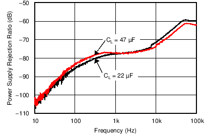
REF6025 REF6030 REF6033 REF6041 REF6045 REF6050 C011_SBOS708.png
Figure 15. PSRR vs Frequency
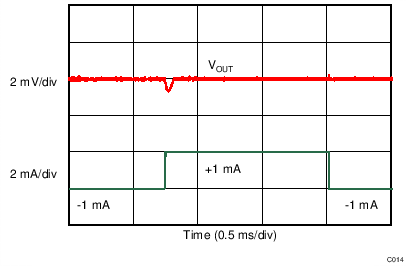
REF6025 REF6030 REF6033 REF6041 REF6045 REF6050 C014_SBOS708.png
Load current = ±1 mA
Figure 17. Load Transient Response
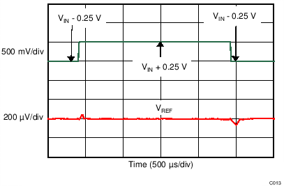
REF6025 REF6030 REF6033 REF6041 REF6045 REF6050 C013_SBOS708.png
Figure 19. Line Transient Response
REF6025 REF6030 REF6033 REF6041 REF6045 REF6050 C027_SBOS708.png
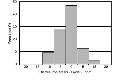
Figure 21. Thermal Hysteresis Distribution (Cycle 2)
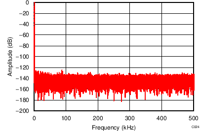
REF6025 REF6030 REF6033 REF6041 REF6045 REF6050 C024_SBOS708.png
REF6050 driving REF pin of ADS8881,
fIN = 1 kHz, SNR = 100.5 dB, THD = –125.9 dB
Figure 23. Typical FFT Plot
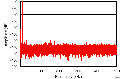
REF6025 REF6030 REF6033 REF6041 REF6045 REF6050 C038_SBOS708.png
REF6050 driving REF pin of ADS8881,
fIN = 10 kHz, SNR = 99.2 dB, THD = –119.4 dB
Figure 25. Typical FFT Plot
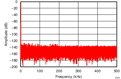
REF6025 REF6030 REF6033 REF6041 REF6045 REF6050 C031_SBOS708.png
REF6041 driving REF pin of ADS8881,
fIN = 2 kHz, SNR = 99 dB, THD = –123.6 dB
Figure 27. Typical FFT Plot
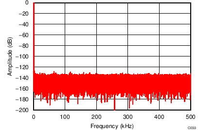
REF6025 REF6030 REF6033 REF6041 REF6045 REF6050 C033_SBOS708.png
REF6025 driving REF pin of ADS8881,
fIN = 1 kHz, SNR = 95.4 dB, THD = –124 dB
Figure 29. Typical FFT Plot
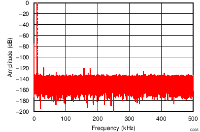
REF6025 REF6030 REF6033 REF6041 REF6045 REF6050 C035_SBOS708.png
REF6025 driving REF pin of ADS8881,
fIN = 10 kHz, SNR = 94.0 dB, THD = –119.3 dB
Figure 31. Typical FFT Plot
REF6025 REF6030 REF6033 REF6041 REF6045 REF6050 C048_SBOS708.png
REF6050 driving REF pin of ADS8881 operating at 1 MSPS,
negative full-scale input to ADS8881
Figure 33. Reference Droop
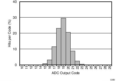
REF6025 REF6030 REF6033 REF6041 REF6045 REF6050 C050_SBOS708.png
AINP = AINN = VREF / 2 for ADS8881,
sampling rate = 1 MSPS
Figure 35. DC Input Histogram
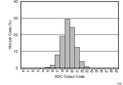
REF6025 REF6030 REF6033 REF6041 REF6045 REF6050 C052_SBOS708.png
AINP = AINN = VREF / 2 for ADS8881,
sampling rate = 100 kSPS
Figure 37. DC Input Histogram
REF6025 REF6030 REF6033 REF6041 REF6045 REF6050 C042_SBOS708.png
1 LSB = 19.07 µV, with ADS8881 at 1 MSPS
Figure 39. Reference Droop Comparison
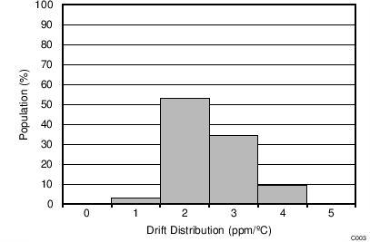
REF6025 REF6030 REF6033 REF6041 REF6045 REF6050 C003_SBOS708.png
TA = –40°C to +85°C
Figure 2. Drift Distribution
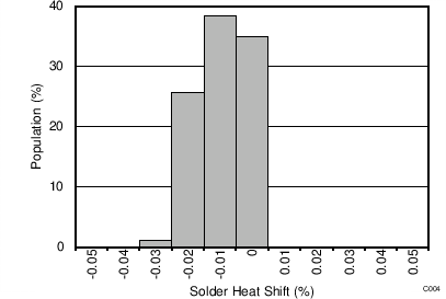
REF6025 REF6030 REF6033 REF6041 REF6045 REF6050 C004_SBOS708.png
Figure 4. Solder-Heat Shift Distribution
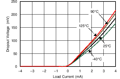
REF6025 REF6030 REF6033 REF6041 REF6045 REF6050 C017_SBOS708.png
Figure 6. Dropout Voltage vs Load Current
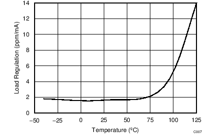
REF6025 REF6030 REF6033 REF6041 REF6045 REF6050 C007_SBOS708.png
VIN = VOUT + 600 mV,
IL = 0 mA to 4 mA
Figure 8. Load Regulation Sinking vs Temperature
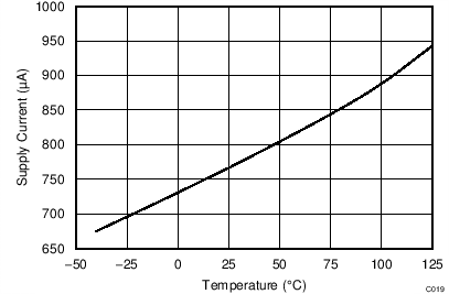
REF6025 REF6030 REF6033 REF6041 REF6045 REF6050 C019_SBOS708.png
Figure 10. Supply Current vs Temperature
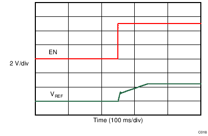
REF6025 REF6030 REF6033 REF6041 REF6045 REF6050 C018_SBOS708.png
Figure 12. Turn-On Settling Time
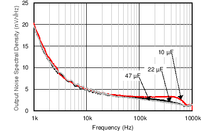
REF6025 REF6030 REF6033 REF6041 REF6045 REF6050 C022_SBOS708.png
Figure 14. Output-Voltage Noise Spectrum
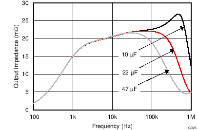
REF6025 REF6030 REF6033 REF6041 REF6045 REF6050 C025_SBOS708.png
Graph obtained by design simulation
Figure 16. Output Impedance vs Frequency
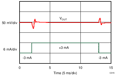
REF6025 REF6030 REF6033 REF6041 REF6045 REF6050 C015_SBOS708.png
Load current = ±3 mA
Figure 18. Load Transient Response
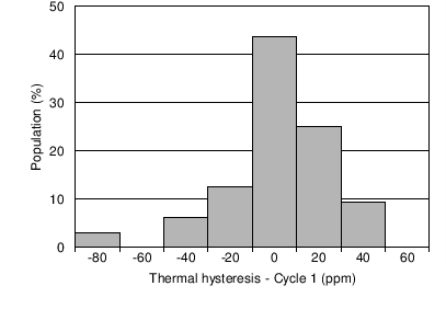
REF6025 REF6030 REF6033 REF6041 REF6045 REF6050 C028_SBOS708.png
Figure 20. Thermal Hysteresis Distribution (Cycle 1)
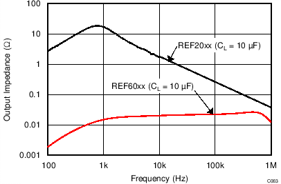
REF6025 REF6030 REF6033 REF6041 REF6045 REF6050 C063_SBOS708.png
Figure 22. Output Impedance Comparison
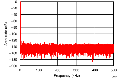
REF6025 REF6030 REF6033 REF6041 REF6045 REF6050 C037_SBOS708.png
REF6050 driving REF pin of ADS8881,
fIN = 2 kHz, SNR = 100.4 dB, THD = –123.9 dB
Figure 24. Typical FFT Plot
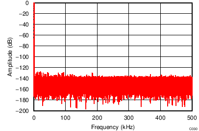
REF6025 REF6030 REF6033 REF6041 REF6045 REF6050 C030_SBOS708.png
REF6041 driving REF pin of ADS8881,
fIN = 1 kHz, SNR = 99 dB, THD = –124.4 dB
Figure 26. Typical FFT Plot
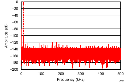
REF6025 REF6030 REF6033 REF6041 REF6045 REF6050 C032_SBOS708.png
REF6041 driving REF pin of ADS8881,
fIN = 10 kHz, SNR = 97.2 dB, THD = –119.7 dB
Figure 28. Typical FFT Plot
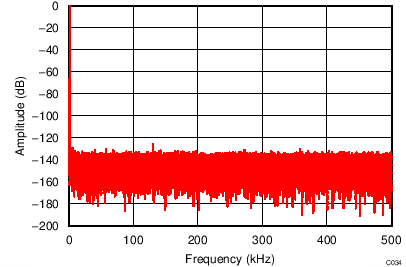
REF6025 REF6030 REF6033 REF6041 REF6045 REF6050 C034_SBOS708.png
REF6025 driving REF pin of ADS8881,
fIN = 2 kHz, SNR = 95.4 dB, THD = –123.5 dB
Figure 30. Typical FFT Plot
REF6025 REF6030 REF6033 REF6041 REF6045 REF6050 C047_SBOS708.png
REF6050 driving REF pin of ADS8881 operating at 1 MSPS,
positive full-scale input to ADS8881
Figure 32. Reference Droop
REF6025 REF6030 REF6033 REF6041 REF6045 REF6050 C049_SBOS708.png
REF6050 driving REF pin of ADS8881 operating at 1 MSPS,
AINP = AINN = VREF / 2 for ADS8881
Figure 34. Reference Droop
REF6025 REF6030 REF6033 REF6041 REF6045 REF6050 C051_SBOS708.png
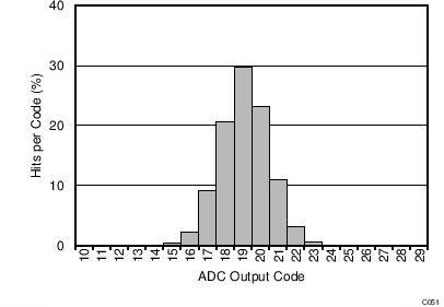
AINP = AINN = VREF / 2 for ADS8881,
sampling rate = 500 kSPS
Figure 36. DC Input Histogram
REF6025 REF6030 REF6033 REF6041 REF6045 REF6050 C053_SBOS708.png
AINP = AINN = VREF / 2 for ADS8881,
sampling rate = 20 kSPS
Figure 38. DC Input Histogram