SBOS708B May 2016 – August 2016 REF6025 , REF6030 , REF6033 , REF6041 , REF6045 , REF6050
PRODUCTION DATA.
- 1 Features
- 2 Applications
- 3 Description
- 4 Revision History
- 5 Device Comparison Table
- 6 Pin Configuration and Functions
- 7 Specifications
- 8 Parameter Measurement Information
- 9 Detailed Description
- 10Applications and Implementation
- 11Power Supply Recommendations
- 12Layout
- 13Device and Documentation Support
- 14Mechanical, Packaging, and Orderable Information
Package Options
Mechanical Data (Package|Pins)
- DGK|8
Thermal pad, mechanical data (Package|Pins)
Orderable Information
9.3.4 Stability
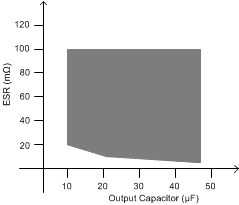
The REF60xx family of voltage references are stable with output capacitor values ranging from 10 µF to 47 µF. At a low output-capacitor value of 10 µF, an effective series resistance (ESR) of 20 mΩ to 100 mΩ is required for stability; whereas, at a higher value of 47 µF, an ESR of 5 mΩ to 100 mΩ is required. The shaded region in Figure 53 shows the stable region of operation for the REF60xx devices.
 Figure 53. Stable Output Capacitor Range
A capacitor of value 1 µF is required at the FILT pin for stability and noise performance. A low ESR (5 mΩ to 20 mΩ) is easily achieved by increasing the PCB trace length, thus eliminating the need for a discrete resistor. Higher values of ESR (greater than 20 mΩ, but lesser than 100 mΩ) can be intentionally added to increase the output bandwidth of the REF60xx. This higher ESR improves the transient performance of the REF60xx, but worsens noise performance because of increased bandwidth.