SLAS834C November 2012 – December 2014 RF430FRL152H , RF430FRL153H , RF430FRL154H
PRODUCTION DATA.
- 1Device Overview
- 2Revision History
- 3Device Comparison
- 4Terminal Configuration and Functions
-
5Specifications
- 5.1 Absolute Maximum Ratings
- 5.2 ESD Ratings
- 5.3 Recommended Operating Conditions
- 5.4 Recommended Operating Conditions, Resonant Circuit
- 5.5 Active Mode Supply Current Into VDDB Excluding External Current
- 5.6 Low-Power Mode Supply Current (Into VDDB) Excluding External Current
- 5.7 Digital I/Os (P1, RST/NMI)
- 5.8 High-Frequency Oscillator (4 MHz), HFOSC
- 5.9 Low-Frequency Oscillator (256 kHz), LFOSC
- 5.10 Wake-Up From Low-Power Modes
- 5.11 Timer_A
- 5.12 eUSCI (SPI Master Mode) Recommended Operating Conditions
- 5.13 eUSCI (SPI Master Mode)
- 5.14 eUSCI (SPI Slave Mode)
- 5.15 eUSCI (I2C Mode)
- 5.16 FRAM
- 5.17 JTAG
- 5.18 RFPMM, Power Supply Switch
- 5.19 RFPMM, Bandgap Reference
- 5.20 RFPMM, Voltage Doubler
- 5.21 RFPMM, Voltage Supervision
- 5.22 SD14, Performance
- 5.23 SVSS Generator
- 5.24 Thermistor Bias Generator
- 5.25 Temperature Sensor
- 5.26 RF13M, Power Supply and Recommended Operating Conditions
- 5.27 RF13M, ISO/IEC 15693 ASK Demodulator
- 5.28 RF13M, ISO/IEC 15693 Compliant Load Modulator
-
6Detailed Description
- 6.1 CPU
- 6.2 Instruction Set
- 6.3 Operating Modes
- 6.4 Interrupt Vector Addresses
- 6.5 Memory
- 6.6
Peripherals
- 6.6.1 Digital I/O, (P1.x)
- 6.6.2 Versatile I/O Port P1
- 6.6.3 Oscillator and System Clock
- 6.6.4 Compact System Module (C-SYS_A)
- 6.6.5 Watchdog Timer (WDT_A)
- 6.6.6 Reset, NMI, SVMOUT System
- 6.6.7 Timer_A (Timer0_A3)
- 6.6.8 Enhanced Universal Serial Communication Interface (eUSCI_B0)
- 6.6.9 ISO/IEC 15693 Analog Front End (RF13M)
- 6.6.10 ISO/IEC 15693 Decoder/Encoder (RF13M)
- 6.6.11 CRC16 Module (CRC16)
- 6.6.12 14-Bit Sigma-Delta ADC (SD14)
- 6.6.13 Programmable Gain Amplifier (SD14)
- 6.6.14 Peripheral Register Map
- 6.7 Port Schematics
- 6.8 Device Descriptors (TLV)
- 7Applications, Implementation, and Layout
- 8Device and Documentation Support
- 9Mechanical Packaging and Orderable Information
Package Options
Mechanical Data (Package|Pins)
- RGE|24
Thermal pad, mechanical data (Package|Pins)
- RGE|24
Orderable Information
6 Detailed Description
6.1 CPU
The MSP430 CPU has a 16-Bit RISC architecture that is highly transparent to the application. All operations, other than program-flow instructions, are performed as register operations in conjunction with seven addressing modes for source operand and four addressing modes for destination operand.
The CPU is integrated with 16 registers that provide reduced instruction execution time. The register-to-register operation execution time is one cycle of the CPU clock.
Four of the registers, R0 to R3, are dedicated as program counter, stack pointer, status register, and constant generator respectively. The remaining registers are general-purpose registers.
Peripherals are connected to the CPU using data, address, and control buses, and can be handled with all instructions.
6.2 Instruction Set
The instruction set consists of the original 51 instructions with three formats and seven address modes. Each instruction can operate on word and byte data.
6.3 Operating Modes
The device has one active mode and three software selectable low-power modes of operation. An interrupt event can wake up the device from any of the three low-power modes, service the request, and restore back to the low-power mode on return from the interrupt program.
NOTE
The software-selected low-power mode might not be reached if at least one module still requests a clock on MCLK, SMCLK, or ACLK. The CPU, however, remains off until an interrupt occurs.
The following operating modes can be configured by software:
- Active mode AM
- CPU is enabled
- All clocks are active.
- Low-power mode 0 (LPM0)
- CPU is disabled
- MCLK is disabled
- SMCLK is active
- ACLK is active
- HFOSC is off, if not selected for SMCLK or ACLK
- Low-power mode 3 (LPM3)
- CPU is disabled
- MCLK is disabled
- SMCLK is disabled
- ACLK is active
- HFOSC is off, if not selected for ACLK
- Low-power mode 4 (LPM4)
- CPU is disabled
- MCLK is disabled
- SMCLK is disabled
- ACLK is disabled
- HFOSC is off, LFOSC is on
LPM1 is identical to LPM0, and LPM2 is identical to LPM3, because the SCG0 bit has no influence on HFOSC.
6.4 Interrupt Vector Addresses
The interrupt vectors and the power-up start address are located in the address range 0FFFFh to 0FFE0h. Address Range 0FFDFh to 0FFD0h is reserved for bootcode signatures. The vector contains the 16-bit address of the appropriate interrupt-handler instruction sequence.
Table 6-1 Interrupt Sources, Flags, and Vectors
| INTERRUPT SOURCE | INTERRUPT FLAG | SYSTEM INTERRUPT | WORD ADDRESS | PRIORITY |
|---|---|---|---|---|
|
System Reset Power-Up External Reset Watchdog |
WDTIFG(1) | Reset | FFFEh | 15, highest |
|
System NMI Vacant memory access |
SVMIFG, VMAIFG(1) | (Non)maskable | 0FFFCh | 14 |
|
User NMI NMI |
NMIIFG(1)(2) | (Non)maskable | 0FFFAh | 13 |
| TimerA0_A3 | TA0CCR0 CCIFG0(3) | Maskable | 0FFF8h | 12 |
| TimerA0_A3 | TA0CCR1 CCIFG1 TA0CCR2 CCIFG2 TA0CTL TAIFGTA0IV(1)(3) |
Maskable | 0FFF6h | 11 |
| Watchdog, Interval Timer Mode |
WDTIFG | Maskable | 0FFF4h | 10 |
| RF13M Module | RF13MRXIFG, RF13MTXIFG, RF13MRXWMIFG, RF13MTXWMIFG, RF13MSLIFG, RF13MOUFLIFG, RF13MRXEIFG, RF13MIVx(1)(3) | Maskable | 0FFF2h | 9 |
| eUSCIB |
(SPI mode) UCB0ALIFG, UCB0NACKIFG, UCB0STTIFG, UCB0STPIFG, UCB0RXIFG3, UCB0TXIFG3, UCB0RXIFG2, UCB0TXIFG2, UCB0RXIFG1, UCB0TXIFG1, UCB0RXIFG0, UCB0TXIFG0, UCB0CNTIFG, UCB0CLTOIFG, UCB0BIT9IFG |
Maskable | 0FFF0h | 8 |
| Sigma Delta ADC | SD14OVIFG, SD14IFG(1)(3) | Maskable | 0FFEEh | 7 |
| I/O Port P1 | P1IFG.0 to P1IFG.7 (P1IV)(1)(3) |
Maskable | 0FFECh | 6 |
| RFPMM | RFPMMIFGV2X, RFPMMIFGVH, RFPMMIFGVR, RFPMMIFGVB, RFPMMIFGVF, RFPMMIV | Maskable | 0FFEAh | 5 |
| Reserved | Reserved(4) | 0FFE8h | 4 | |
| ⋮ | ⋮ | |||
| 0FFDCh | 0 | |||
| Signatures | CRC Value | 0FFDAh | ||
| CRC Length | 0FFD8h | |||
| Loader Signature 1 | 0FFD6h | |||
| Loader Signature 0 | 0FFD4h | |||
| JTAG Signature 1 | 0FFD2h | |||
| JTAG Signature 0 | 0FFD0h |
(Non)maskable: the individual interrupt-enable bit can disable an interrupt event, but the general-interrupt enable cannot disable it.
6.5 Memory
Table 6-2 shows the memory organization of the devices.
Table 6-2 Memory Map RF430FRL152H, RF430FRL153H, RF430FRL154H
| TYPE | RF430FRL152H RF430FRL153H RF430FRL154H Normal Mode |
RF430FRL152H RF430FRL153H RF430FRL154H ROM Development Mode |
|
|---|---|---|---|
| Memory (FRAM) Main: interrupt vector |
Total Size FRAM |
2048 B = 2 KB 0FFFFh-0FFE0h |
|
| Main: Code Memory | Bank A(1)(2) | 512 B 0FFFFh-0FE00h |
|
| Bank B(1) | 512 B 0FDFFh-0FC00h |
||
| Bank C(1) | 512 B 0FBFFh-0FA00h |
||
| Bank D | 448 B 0F9FFh-0F840h |
||
| Boot Data (TLV) | Size FRAM |
64 B 01A3Fh-01A00h |
64 B 01A3Fh-01A00h |
| Application ROM | Size ROM |
7168 B = 7 KB 05FFFh-04400h |
3584 B = 3.5 KB 051FFh-04400h |
| ROM Development Memory | Size SRAM |
- - |
3584 B = 3.5 KB 02BFFh-01E00h |
| SRAM Memory | Size SRAM |
4096 B = 4 KB 02BFFh-01C00h |
512 B = 0.5 KB 01DFFh-01C00h |
| Peripherals | Size | 4096 B = 4 KB 00FFFh-00000h |
4096 B = 4 KB 00FFFh-00000h |
6.5.1 FRAM
The FRAM can be programmed through the JTAG port or in-system by the CPU, data are received through RF, SPI or I2C Sensor Interface.
Features of the FRAM include:
- Low-power ultra-fast-write non-volatile memory
- Byte and word access capability
- Automated wait state generation
The following address ranges can be write protected by setting the corresponding bit in the SYSCNF register, see the RF430FRL15xH Family Technical Reference Manual (SLAU506).
Table 6-3 Write Protectable FRAM Address Ranges
| BIT | Address Range |
|---|---|
| FRAMLCK2 | 512 B 0FFFFh-0FE00h |
| FRAMLCK1 | 512 B 0FDFFh-0FC00h |
| FRAMLCK0 | 512 B 0FBFFh-0FA00h |
6.5.2 SRAM
The SRAM memory is made up of 8 sectors. Each sector can be completely powered down to save leakage; however, all data is lost. Features of the SRAM memory include:
- SRAM memory has 8 sectors of 512 B each.
- Each sector 0 to 8 can be complete disabled; however, data retention is lost.
- Each sector 0 to 8 automatically enters low-power retention mode when possible.
6.5.3 Application ROM
The Application ROM consists of four parts. The RF Library provides ISO/IEC 15693 functions necessary for operating the 13.65 MHz front end. The Function library holds the device and memory function used by the boot code and RF library. These functions are user accessible. The ROM contains the predefined application FW. The boot code checks the password and releases control to the application or enables JTAG on password match, enters LPM4 and waits for debug session, see the RF430FRL15xH Firmware User's Guide (SLAU603).
6.6 Peripherals
Peripherals are connected to the CPU through data, address, and control buses. All peripherals can be managed using all instructions. For complete module descriptions, see the RF430FRL15xH Family Technical Reference Manual (SLAU506).
6.6.1 Digital I/O, (P1.x)
There is one I/O port implemented, P1, with eight I/O lines RF430FRL15xH.
- All individual I/O bits are independently programmable.
- Any combination of input, output, and interrupt conditions is possible.
- Programmable pullup or pulldown resistor on all ports.
- Edge-selectable interrupt input capability for all ports on P1.
- Read and write access to port-control registers is supported by all instructions.
6.6.2 Versatile I/O Port P1
The versatile I/O ports P1 feature device dependent reset values. The reset values for the RF430FRL15xH devices are shown in Table 6-4.
Table 6-4 Versatile Port Reset Values
| PORT NUMBER | PxOUT | PxDIR | PxREN | PxSEL0 | PxSEL1 | RESET | PORTS ON | COMMENT |
|---|---|---|---|---|---|---|---|---|
| P1.0 | 0 | 0 | 0 | 0 | 0 | PUC | yes | P1.0, input |
| P1.1 | 0 | 0 | 0 | 0 | 0 | PUC | yes | P1.1, input |
| P1.2 | 0 | 0 | 0 | 0 | 0 | PUC | yes | P1.2, input |
| P1.3 | 0 | 0 | 0 | 0 | 0 | PUC | yes | P1.3, input |
| P1.4 | 1 | 0 | 1 | 1 | 1 | PUC | yes | JTAG TCK, P1.4, input |
| P1.5 | 1 | 0 | 1 | 1 | 1 | PUC | yes | JTAG TDI, P1.5, input |
| P1.6 | 0 | 0 | 0 | 1 | 1 | PUC | yes | JTAG TDO, P1.6, output |
| P1.7 | 1 | 0 | 1 | 1 | 1 | PUC | yes | JTAG TMS, P1.7, input |
6.6.3 Oscillator and System Clock
The clock system in the RF430FRL15xH devices is supported by the Compact Clock System (CCS) module that includes support for an internal trimmable 256-kHz current-controlled low-frequency oscillator (LFOSC) and an internal 4-MHz current-controlled high-frequency oscillator (HFOSC).
The CCS module is designed to meet the requirements of both low system cost and low power consumption. The CCS provides a fast turn-on of the oscillators in less than 1 ms. The CCS module provides the following clock signals:
- Auxiliary clock (ACLK), sourced from the 256-kHz internal LFOSC.
- Main clock (MCLK), the system clock used by the CPU. MCLK can be sourced by same sources made available to ACLK.
- Sub-Main clock (SMCLK), the subsystem clock used by the peripheral modules. SMCLK can be sourced by same sources made available to ACLK.
6.6.4 Compact System Module (C-SYS_A)
The Compact SYS module handles many of the system functions within the device. These include power-on reset and power-up clear handling, NMI source selection and management, reset interrupt vector generators, as well as, configuration management. It also includes a data exchange mechanism through JTAG called a JTAG mailbox that can be used in the application.
Table 6-5 System Module Interrupt Vector Registers
| INTERRUPT VECTOR REGISTER | INTERRUPT VECTOR | WORD ADDRESS | OFFSET | PRIORITY |
|---|---|---|---|---|
| SYSRSTIV, System Reset | No interrupt pending | 019Eh | 00h | |
| Brownout (BOR) | 02h | Highest | ||
| SVMBOR (BOR) | 04h | |||
| RST/NMI (BOR) | 06h | |||
| DoBOR (BOR) | 08h | |||
| Security violation (BOR) | 0Ah | |||
| DoPOR (POR) | 0Ch | |||
| WDT time-out (PUC) | 0Eh | |||
| WDT key violation (PUC) | 10h | |||
| CCS key violation | 12h | |||
| PMM key violation | 14h | |||
| Peripheral area fetch (PUC) | 16h | |||
| Reserved | 18h-3Eh | Lowest | ||
| SYSSNIV, System NMI | No interrupt pending | 019Ch | 00h | |
| SVMIFG | 02h | Highest | ||
| VMAIFG | 04h | |||
| JMBINIFG | 06h | |||
| JMBOUTIFG | 08h | |||
| Reserved | 0Ah-3Eh | Lowest | ||
| SYSUNIV, User NMI | No interrupt pending | 019Ah | 00h | |
| NMIFG | 02h | Highest | ||
| OFIFG | 04h | |||
| BERR | 06h | |||
| Reserved | 08h-3Eh | Lowest | ||
| SYSBERRIV, Bus Error | No interrupt pending | 0198h | 00h | |
| Reserved | 02h-3Eh | Lowest |
6.6.5 Watchdog Timer (WDT_A)
The primary function of the watchdog timer (WDT_A) module is to perform a controlled system restart after a software problem occurs. If the selected time interval expires, a system reset is generated. If the watchdog function is not needed in an application, the module can be configured as an interval timer and can generate interrupts at selected time intervals.
6.6.6 Reset, NMI, SVMOUT System
The reset system of the RF430FRL15xH devices features the function reset input, reset output, and NMI input.
6.6.7 Timer_A (Timer0_A3)
Timer_A is a 16-bit timer/counter with three capture/compare registers. Timer_A can support multiple capture/compares, PWM outputs, and interval timing. Timer_A also has extensive interrupt capabilities. Interrupts may be generated from the counter on overflow conditions and from each of the capture/compare registers.
Table 6-6 Timer0_A3 Signal Connections
| INPUT PIN NUMBER | DEVICE INPUT SIGNAL | MODUL INPUT SIGNAL | MODULE BLOCK | MODULE OUTPUT SIGNAL | DEVICE OUTPUT SIGNAL | OUTPUT PIN NUMBER |
|---|---|---|---|---|---|---|
| 8 – P1.3 | TA0CLK | TACLK | Timer | NA | NA | |
| ACLK (internal) | ACLK | |||||
| SMCLK (internal) | SMCLK | |||||
| TA0CLK | TACLK | |||||
| 12 – P1.0 | TA0.0 | CCI0A | CCR0 | TA0 | TA0.0 | 9 – P1.2 |
| 11 – P1.1 | TA0.0 | CCI0B | 20 – P1.6 | |||
| VSS | GND | 19 – P1.7 | ||||
| VDDB | Vcc | |||||
| 22 – P1.4 | TA0.1 | CCI1A | CCR1 | TA1 | TA0.1 | 12 – P1.0 |
| 21 – P1.5 | TA0.1 | CCI1B | 22 – P1.4 | |||
| VSS | GND | 19 – P1.7 | ||||
| VDDB | Vcc | |||||
| 20 – P1.6 | TA0.2 | CCI2A | CCR2 | TA2 | TA0.2 | 11 – P1.1 |
| 19 – P1.7 | TA0.2 | CCI2B | 8 – P1.3 | |||
| VSS | GND | 21 – P1.5 | ||||
| VDDB | Vcc | 20 – P1.6 |
6.6.8 Enhanced Universal Serial Communication Interface (eUSCI_B0)
The eUSCI_B0 module is used for serial data communication. The eUSCI module supports synchronous communication protocols such as SPI (3 pin or 4 pin) and I2C.
The eUSCI_B0 module provides support for SPI (3 pin or 4 pin) or I2C.
6.6.9 ISO/IEC 15693 Analog Front End (RF13M)
The ISO/IEC 15693 module supports contact-less communication over the analog front end according to ISO/IEC 15693 with data rates up to 26.48 kbps for receive and 26.48 kbps for transmit. It includes decode of receive data and encode of transmit data, both synchronous with the AFE carrier clock.
6.6.10 ISO/IEC 15693 Decoder/Encoder (RF13M)
The module interfaces directly to the analog front end to ensure correct timing for transmit and receive of data derived from the 13.56-MHz carrier frequency.
6.6.11 CRC16 Module (CRC16)
The CRC16 module produces a signature based on a sequence of entered data values and can be used for data
checking purposes. The CRC16 module is compliant with ISO/IEC 13239, it is 16 bits long, polynominal is: x16 + x12 + x5 + 1, direction is backward, and preset is 0xFFFF. For more information see ISO/IEC 13239.
6.6.12 14-Bit Sigma-Delta ADC (SD14)
A sigma-delta modulator is provided for high resolution analog-to-digital conversion of quasi-dc voltages:
- First-order integrator, 1-bit comparator, 1-bit DAC
- Sampling frequency of up to 2 kHz
- Fully differential
6.6.13 Programmable Gain Amplifier (SD14)
The PGA features a very high-impedance input and a programmable gain combined with full offset compensation, very low offset drift, and low noise.
6.6.14 Peripheral Register Map
Table 6-7 Peripheral Register Map
| MODULE NAME | REGISTER DESCRIPTION | REGISTER | BASE ADDRESS | OFFSET |
|---|---|---|---|---|
| RF13M | RF13M RX/TX High/Low Watermark Configuration Register | RF13MWMCFG | 0800h | 0Eh |
| RF13M RX/TX FIFO Fill Level register | RF13MFIFOFL | 0Ch | ||
| RF13M CRC accumulator Register | RF13MCRC | 0Ah | ||
| RF13M Transmit Data FIFO Register | RF13MTXF | 08h | ||
| RF13M Receive Data FIFO Register | RF13MRXF | 06h | ||
| RF13M Interrupt Vector Register | RF13MIV | 04h | ||
| RF13M Interrupt Register | RF13MINT | 02h | ||
| RF13M Control Register | RF13MCTL | 00h | ||
| SD14 | SD14 Interrupt Vector Register | SD14IV | 0700h | 0Ch |
| SD14 Intermediate Conversion Result Register | SD14MEM3 | 0Ah | ||
| SD14 Intermediate Conversion Result Register | SD14MEM2 | 08h | ||
| SD14 Intermediate Conversion Result Register | SD14MEM1 | 06h | ||
| SD14 Conversion Result | SD14MEM0 | 04h | ||
| SD14 Control Register 1 | SD14CTL1 | 02h | ||
| SD14 Control Register 0 | SD14CTL0 | 00h | ||
| eUSCI_B0 | Interrupt Vector Word Register | UCB0IV | 0640h | 2Eh |
| Interrupt Flags Register | UCB0IFG | 2Ch | ||
| Interrupt Enable Register | UCB0IE | 2Ah | ||
| I2C Slave Address Register | UCB0I2CSA | 20h | ||
| Address Mask Register | UCB0ADDMASK | 1Eh | ||
| Received Address Register | UCB0ADDRX | 1Ch | ||
| I2C Own Address 3 Register | UCB0I2COA3 | 1Ah | ||
| I2C Own Address 2 Register | UCB0I2COA2 | 18h | ||
| I2C Own Address 1 Register | UCB0I2COA1 | 16h | ||
| I2C Own Address 0 Register | UCB0I2COA0 | 14h | ||
| Transmit Buffer Register | UCB0TXBUF | 0Eh | ||
| Receive Buffer Register | UCB0RXBUF | 0Ch | ||
| Byte Counter Threshold Register | UCB0TBCNT | 0Ah | ||
| Status Word Register | UCB0STATW | 08h | ||
| Bit Rate 1 Register | UCB0BR1 | 07h | ||
| Bit Rate 0 Register | UCB0BR0 | 06h | ||
| Control Word 1 Register | UCB0CTLW1 | 02h | ||
| Control Word 0 Register | UCB0CTLW0 | 00h | ||
| Timer0_A3 | Timer0_A Interrupt Vector Register | TA0IV | 0340h | 2Eh |
| Capture/Compare Register 2 | TA0CCR2 | 16h | ||
| Capture/Compare Register 1 | TA0CCR1 | 14h | ||
| Capture/Compare Register 0 | TA0CCR0 | 12h | ||
| Timer0_A Counter Register | TA0R | 10h | ||
| Capture/Compare Control 2 Register | TA0CCTL2 | 06h | ||
| Capture/Compare Control 1 Register | TA0CCTL1 | 04h | ||
| Capture/Compare Control 0 Register | TA0CCTL0 | 02h | ||
| Timer0_A Control Register | TA0CTL | 00h | ||
| Port P1 | Port P1 Interrupt Flag Register | P1IFG | 0200h | 1Ch |
| Port P1 Interrupt Enable Register | P1IE | 1Ah | ||
| Port P1 Interrupt Edge Select Register | P1IES | 18h | ||
| Port P1 Interrupt Vector Word Register | P1IV | 0Eh | ||
| Port P1 Selection 1 Register | P1SEL1 | 0Ch | ||
| Port P1 Selection 0 Register | P1SEL0 | 0Ah | ||
| Port P1 Pullup/Pulldown Enable Register | P1REN | 06h | ||
| Port P1 Direction Register | P1DIR | 04h | ||
| Port P1 Outout Register | P1OUT | 02h | ||
| Port P1 Input Register | P1IN | 00h | ||
| CSYS_A | Reset Vector Generator Register | SYSRSTIV | 0180h | 1Eh |
| System NMI Vector Generator Register | SYSSNIV | 1Ch | ||
| User NMI Vector Generator Register | SYSUNIV | 1Ah | ||
| Bus Error Vector Generator Register | SYSBERRIV | 18h | ||
| System Configuration Actuator 0 Register | SYSCA0 | 14h | ||
| System Configuration Register | SYSCNF | 10h | ||
| JTAG Mailbox Output Register 1 | SYSJMBO1 | 0Eh | ||
| JTAG Mailbox Output Register 0 | SYSJMBO0 | 0Ch | ||
| JTAG Mailbox Input Register 1 | SYSJMBI1 | 0Ah | ||
| JTAG Mailbox Input Register 0 | SYSJMBI0 | 08h | ||
| JTAG Mailbox Control Register | SYSJMBC | 06h | ||
| System Control Register | SYSCTL | 00h | ||
| CCS | CCS Control 8 Register | CCSCTL8 | 0160h | 10h |
| CCS Control 7 Register | CCSCTL7 | 0Eh | ||
| CCS Control 6Register | CCSCTL6 | 0Ch | ||
| CCS Control 5 Register | CCSCTL5 | 0Ah | ||
| CCS Control 4 Register | CCSCTL4 | 08h | ||
| CCS Control 1 Register | CCSCTL1 | 02h | ||
| CCS Control 0 Register | CCSCTL0 | 00h | ||
| WDT_A, CRC | Watchdog Timer Control Register | WDTCTL | 0150h | 0Ch |
| CRC Result Reverse Register | CRCRESR | 06h | ||
| CRC Initialization and Result Register | CRCINIRES | 04h | ||
| CRC Data In Reverse Byte Register | CRCDIRB | 02h | ||
| CRC Data In Register | CRCDI | 00h | ||
| FRAM Control | General Control 1 Register | GCCTL1 | 0140h | 06h |
| General Control 0 Register | GCCTL0 | 04h | ||
| FRAM Control 0 Register | FRCTL0 | 00h | ||
| RFPMM | RFPMM Interrupt Vector Register | RFPMMIV | 0120h | 08h |
| RFPMM Interrupt Flag Register | RFPMMIFG | 06h | ||
| RFPMM Interrupt Enable Register | RFPMMIE | 04h | ||
| RFPMM Control Register 1 | RFPMMCTL1 | 02h | ||
| RFPMM Control Register 0 | RFPMMCTL0 | 00h | ||
| Special Functions | SFR Reset Pin Control Register | SFRRPCR | 0100h | 04h |
| SFR Interrupt Flag Register | SFRIFG1 | 02h | ||
| SFR Interrupt Enable Register | SFRIE1 | 00h |
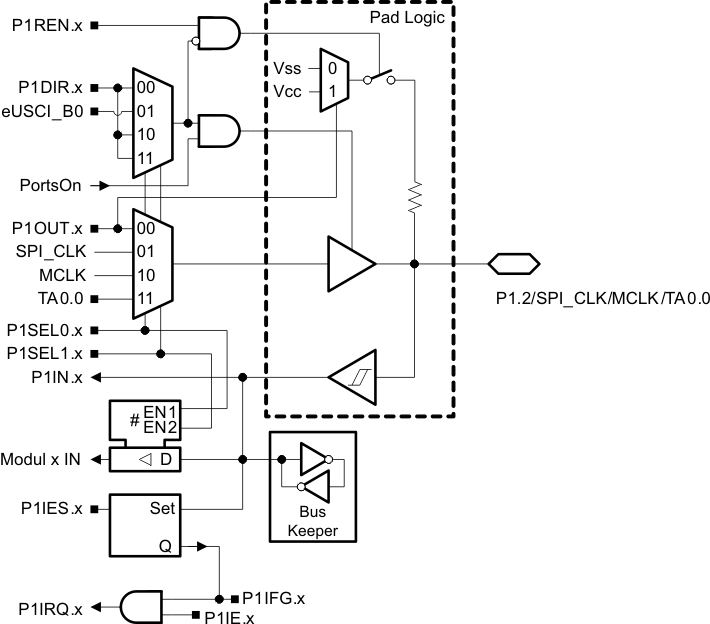
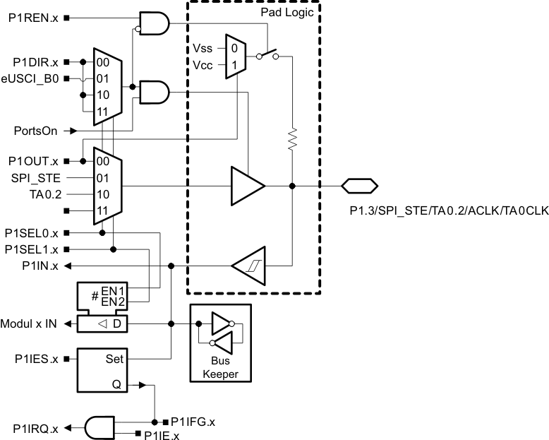
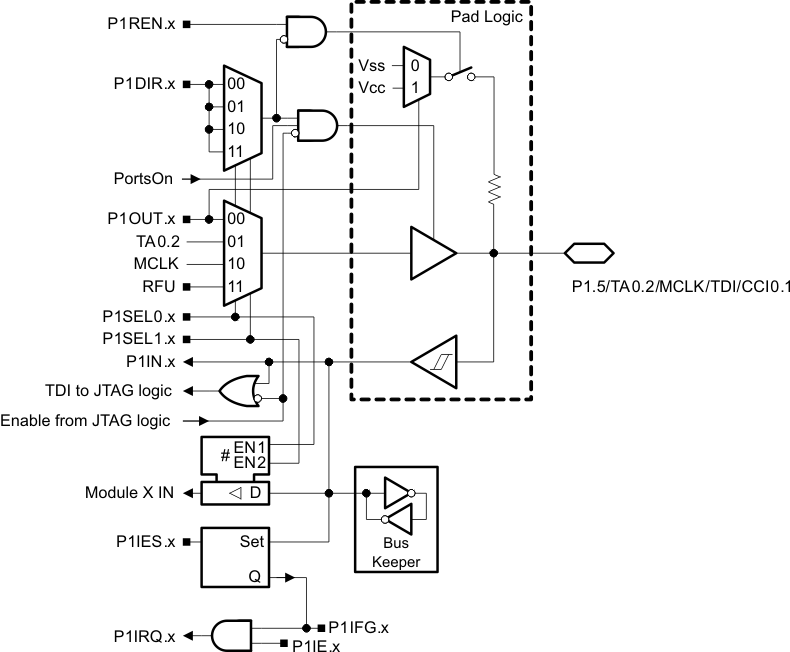
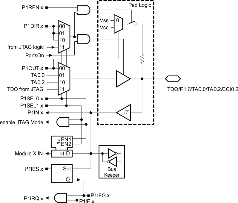
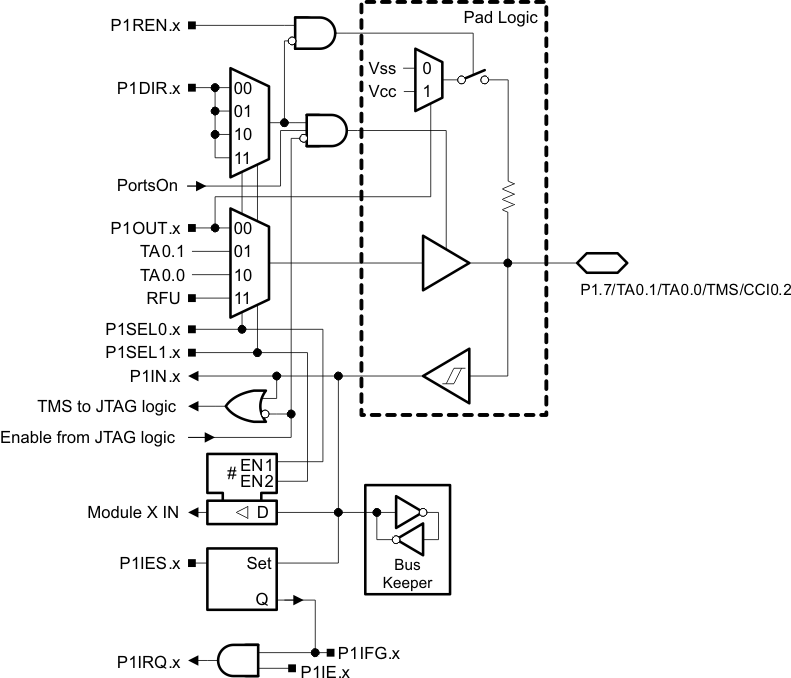
6.7 Port Schematics
6.7.1 Port P1.0 Input/Output

Table 6-8 Port P1.0 Pin Functions
| PIN NAME (P1.x) | x | FUNCTION | CONTROL BITS OR SIGNALS(1) | |||
|---|---|---|---|---|---|---|
| P1DIR.x | P1SEL1.x | P1SEL0.x | RSELx/ ASELx | |||
| P1.0/SPI_SIMO/SDA/SMCLK/TA0.1/CCI0.0 | 0 | P1.0 (I/O) | I:0; O:1 | 0 | 0 | 0 |
| SPI_SIMO/SDA(1) | 1 | 0 | 1 | 0 | ||
| SMCLK | 1 | 1 | 0 | 0 | ||
| TA0.1 | 1 | 1 | 1 | 0 | ||
| Timer A0, CCI0A | 0 | ≠0 | ≠0 | X | ||
6.7.2 Port P1.1 Input/Output
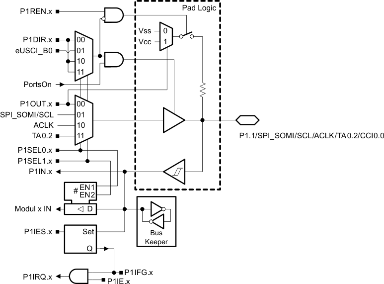
6.7.3 Port P1.2 Input/Output
6.7.4 Port P1.3 Input/Output
6.7.5 Port P1.4 Input/Output
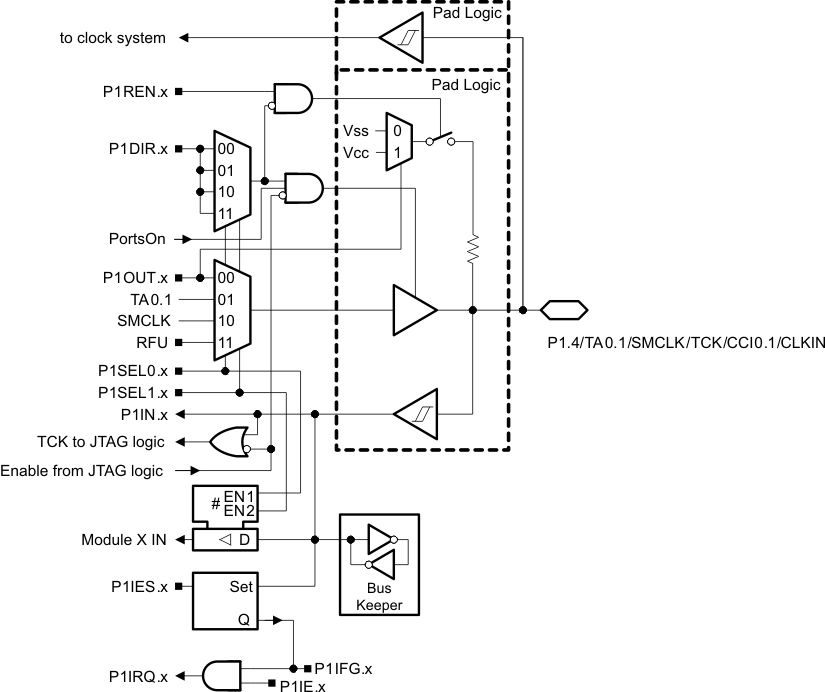
Table 6-12 Port P1.4 Pin Functions
| PIN NAME (P1.x) | x | FUNCTION | CONTROL BITS OR SIGNALS(1) | |||
|---|---|---|---|---|---|---|
| P1DIR.x | P1SEL1.x | P1SEL0.x | JTAG Mode | |||
| TCK/P1.4/TA0.1/SMCLK/CCI0.1 | 4 | P1.4 (I/O) | I:0; O:1 | 0 | 0 | 0 |
| Timer_A0.1 | 1 | 0 | 1 | 0 | ||
| SMCLK | 1 | 1 | 0 | 0 | ||
| Reserved | 1 | 1 | 1 | 0 | ||
| Timer_A0.CCI1A | 0 | ≠0 | ≠0 | 0 | ||
| JTAG-TCK(2)(3)(4) | X | X | X | 1 | ||
| CLKIN from bypass | X | X | X | 0 | ||
6.7.6 Port P1.5 Input/Output
6.7.7 Port P1.6 Input/Output
6.7.8 Port P1.7 Input/Output
6.8 Device Descriptors (TLV)
Table 6-16 list the complete contents of the device descriptor tag-length-value (TLV) structure for each device type.
Table 6-16 RF430FRL15xH Boot Data and Device Descriptor Table
| Description | Address | Size bytes |
FRL152H | FRL153H | FRL154H | |
|---|---|---|---|---|---|---|
| Info Block | Boot Data Length | 01A00h | 1 | 03h | 03h | 03h |
| CRC length | 01A01h | 1 | 03h | 03h | 03h | |
| Boot Data CRC value | 01A02h | 2 | per unit | per unit | per unit | |
| Device ID | 01A04h | 1 | E7h | FBh | FCh | |
| Device ID | 01A05h | 1 | 81h | 81h | 81h | |
| Die Record | Lot #0 | 01A06h | 1 | per unit | per unit | per unit |
| Lot #1 | 01A07h | 1 | per unit | per unit | per unit | |
| UID0 | 01A08h | 1 | per unit | per unit | per unit | |
| UID1 | 01A09h | 1 | per unit | per unit | per unit | |
| UID2 | 01A0Ah | 1 | per unit | per unit | per unit | |
| UID3 | 01A0Bh | 1 | per unit | per unit | per unit | |
| UID4 | 01A0Ch | 1 | per unit | per unit | per unit | |
| UID5 | 01A0Dh | 1 | A2h / A3h | A2h / A3h | A2h / A3h | |
| Lot #2 | 01A0Eh | 1 | per unit | per unit | per unit | |
| Fab ID / Wafer Number | 01A0Fh | 1 | per unit | per unit | per unit | |
| Reserved | 01A10h | 2 | 0FFFFh | 0FFFFh | 0FFFFh | |
| Reserved | 01A12h | 2 | 0FFFFh | 0FFFFh | 0FFFFh | |
| Calibration | Calibration Pointer | 01A14h | 2 | 01A14h | 01A14h | 01A14h |
| Reserved | 01A16h | 2 | per unit | per unit | per unit | |
| Reserved | 01A18h | 2 | per unit | per unit | per unit | |
| Reserved | 01A1Ah | 2 | per unit | per unit | per unit | |
| Reserved | 01A1Ch | 2 | per unit | per unit | per unit | |
| Reserved | 01A1Eh | 2 | per unit | per unit | per unit | |
| ECC | ECC of previous data | 01A3E - 01A20h | 32 | per unit | per unit | per unit |
Table 6-17 UID (Unique Identifier) Definition
| Description | Address | Bit7 | Bit6 | Bit5 | Bit4 | Bit3 | Bit2 | Bit1 | Bit0 |
|---|---|---|---|---|---|---|---|---|---|
| Lot ID 0 | 0x1A06 | LotNr[7] | LotNr[6] | LotNr[5] | LotNr[4] | LotNr[3] | LotNr[2] | LotNr[1] | LotNr[0] |
| Lot ID 1 | 0x1A07 | LotNr[15] | LotNr[14] | LotNr[13] | LotNr[12] | LotNr[11] | LotNr[10] | LotNr[9] | LotNr[8] |
| UID0 | 0x1A08 | TI[7] | TI[6] | TI[5] | TI[4] | TI[3] | TI[2] | TI[1] | TI[0] |
| UID1 | 0x1A09 | TI[15] | TI[14] | TI[13] | TI[12] | TI[11] | TI[10] | TI[9] | TI[8] |
| UID2 | 0x1A0A | TI[23] | TI[22] | TI[21] | TI[20] | TI[19] | TI[18] | TI[17] | TI[16] |
| UID3 | 0x1A0B | TI[31] | TI[30] | TI[29] | TI[28] | TI[27] | TI[26] | TI[25] | TI[24] |
| UID4 | 0x1A0C | TI[39] | TI[38] | TI[37] | TI[36] | TI[35] | TI[34] | TI[33] | TI[32] |
| UID5 | 0x1A0D | 1 | 0 | 1 | 0 | 0 | 0 | 1 | TI[40] |
| Lot ID 2 | 0x1A0E | LotNr[23] | LotNr[22] | LotNr[21] | LotNr[20] | LotNr[19] | LotNr[18] | LotNr[17] | LotNr[16] |
| FabID | 0x1A0F | Wafer[4] | Wafer[3] | Wafer[2] | Wafer[1] | Wafer[0] | FabNr[2] | FabNr[1] | FabNr[0] |