SLAS834C November 2012 – December 2014 RF430FRL152H , RF430FRL153H , RF430FRL154H
PRODUCTION DATA.
- 1Device Overview
- 2Revision History
- 3Device Comparison
- 4Terminal Configuration and Functions
-
5Specifications
- 5.1 Absolute Maximum Ratings
- 5.2 ESD Ratings
- 5.3 Recommended Operating Conditions
- 5.4 Recommended Operating Conditions, Resonant Circuit
- 5.5 Active Mode Supply Current Into VDDB Excluding External Current
- 5.6 Low-Power Mode Supply Current (Into VDDB) Excluding External Current
- 5.7 Digital I/Os (P1, RST/NMI)
- 5.8 High-Frequency Oscillator (4 MHz), HFOSC
- 5.9 Low-Frequency Oscillator (256 kHz), LFOSC
- 5.10 Wake-Up From Low-Power Modes
- 5.11 Timer_A
- 5.12 eUSCI (SPI Master Mode) Recommended Operating Conditions
- 5.13 eUSCI (SPI Master Mode)
- 5.14 eUSCI (SPI Slave Mode)
- 5.15 eUSCI (I2C Mode)
- 5.16 FRAM
- 5.17 JTAG
- 5.18 RFPMM, Power Supply Switch
- 5.19 RFPMM, Bandgap Reference
- 5.20 RFPMM, Voltage Doubler
- 5.21 RFPMM, Voltage Supervision
- 5.22 SD14, Performance
- 5.23 SVSS Generator
- 5.24 Thermistor Bias Generator
- 5.25 Temperature Sensor
- 5.26 RF13M, Power Supply and Recommended Operating Conditions
- 5.27 RF13M, ISO/IEC 15693 ASK Demodulator
- 5.28 RF13M, ISO/IEC 15693 Compliant Load Modulator
-
6Detailed Description
- 6.1 CPU
- 6.2 Instruction Set
- 6.3 Operating Modes
- 6.4 Interrupt Vector Addresses
- 6.5 Memory
- 6.6
Peripherals
- 6.6.1 Digital I/O, (P1.x)
- 6.6.2 Versatile I/O Port P1
- 6.6.3 Oscillator and System Clock
- 6.6.4 Compact System Module (C-SYS_A)
- 6.6.5 Watchdog Timer (WDT_A)
- 6.6.6 Reset, NMI, SVMOUT System
- 6.6.7 Timer_A (Timer0_A3)
- 6.6.8 Enhanced Universal Serial Communication Interface (eUSCI_B0)
- 6.6.9 ISO/IEC 15693 Analog Front End (RF13M)
- 6.6.10 ISO/IEC 15693 Decoder/Encoder (RF13M)
- 6.6.11 CRC16 Module (CRC16)
- 6.6.12 14-Bit Sigma-Delta ADC (SD14)
- 6.6.13 Programmable Gain Amplifier (SD14)
- 6.6.14 Peripheral Register Map
- 6.7 Port Schematics
- 6.8 Device Descriptors (TLV)
- 7Applications, Implementation, and Layout
- 8Device and Documentation Support
- 9Mechanical Packaging and Orderable Information
Package Options
Mechanical Data (Package|Pins)
- RGE|24
Thermal pad, mechanical data (Package|Pins)
- RGE|24
Orderable Information
5 Specifications
5.1 Absolute Maximum Ratings(1)
over recommended ranges of supply voltage and operating free-air temperature (unless otherwise noted)| MIN | MAX | UNIT | |
|---|---|---|---|
| Voltage applied at VDDB referenced to VSS (VAMR) | -0.3 | 1.65 | V |
| Voltage applied at VANT referenced to VSS (VAMR) | -0.3 | 3.6 | V |
| Voltage applied to any pin (references to VSS) | -0.3 | VDDB + 0.3 | V |
| Diode current at any device pin(2) | ±2 | mA | |
| Current derating factor when I/O ports are switched in parallel electrically and logically(3) | 0.9 | ||
| Storage temperature range, Tstg(4)(5)(6) | -40 | 125 | °C |
(1) Stresses beyond those listed under Absolute Maximum Ratings may cause permanent damage to the device. These are stress ratings only, and functional operation of the device at these or any other conditions beyond those indicated under Recommended Operating Conditions is not implied. Exposure to absolute-maximum-rated conditions for extended periods may affect device reliability.
(2) All voltages are referenced to VSS.
(3) The diode current increases to ±4.5 mA when two pins are connected, it increases to ±6.75 mA when three pins are connected, and so on.
(4) Soldering during board manufacturing must follow the current JEDEC J-STD-020 specification with peak reflow temperatures not higher than classified on the device label on the shipping boxes or reels. If hand soldering is required for application prototyping, peak temperature must not exceed 250°C for a total of 5 minutes for any single device.
(5) Data retention on FRAM memory cannot be ensured when exceeding the specified maximum storage temperature, Tstg.
(6) Programming of devices with user application code should only be performed after reflow or hand soldering. Factory programmed information, such as calibration values, are designed to withstand the temperatures reached in the current JEDEC J-STD-020 specification.
5.2 ESD Ratings
| VALUE | UNIT | ||||
|---|---|---|---|---|---|
| VESD | Electrostatic discharge (ESD) performance | Human body model (HBM), per ANSI/ESDA/JEDEC JS001(1)(2) | ±2000 | V | |
(1) JEDEC document JEP155 states that 500-V HBM allows safe manufacturing with a standard ESD control process.
(2) Low leakage pin: ADC0 has reduced ESD tolerance of ±500 V HBM.
5.3 Recommended Operating Conditions
Typical data are based on VDDB = 1.5 V, TA = 25°C (unless otherwise noted)| MIN | NOM | MAX | UNIT | ||
|---|---|---|---|---|---|
| VDDB | Supply voltage during program execution | 1.45 | 1.65 | V | |
| VSS | Supply voltage (GND reference) | 0 | V | ||
| TA | Operating free-air temperature | 0 | 70 | °C | |
| CVDDB | Capacitor on VDDB(1) | 100 | nF | ||
| CVDDSW | Capacitor on VDDSW(1) | 2.2 | µF | ||
| CFLY | Charge pump capacitor between CP1 and CP2. Recommended ratio between CFLY and CVDD2X is ≥ 1:10. (1) |
10 | nF | ||
| CVDD2X | Capacitor on VDD2x. Recommended ratio between CFLY and CVDD2X is ≥ 1:10.(1) |
100 | nF | ||
| CVDDD | Capacitor on VDDD(1) | 1 | µF | ||
| CSVSS | Capacitor between SVSS and VSS(1) | 1 | µF | ||
| fSYSTEM | System frequency(2)(3) | 2 | MHz | ||
| fCLKIN | External clock input frequency | 32 | kHz | ||
(1) Low equivalent series resistance (ESR) capacitor
(2) The MSP430 CPU is clocked directly with MCLK. Both the high and low phase of MCLK must not exceed the pulse duration of the specified maximum frequency.
(3) Modules may have a different maximum input clock specification. See the specification of the respective module in this data sheet.
5.4 Recommended Operating Conditions, Resonant Circuit
| MIN | NOM | MAX | UNIT | ||
|---|---|---|---|---|---|
| fc | Carrier frequency | 13.56 | MHz | ||
| VANT_peak | Antenna input voltage | 3.6 | V | ||
| Z | Impedance of LC circuit | 6.5 | 15.5 | kΩ | |
| LRES | Coil inductance | 2.66 | µH | ||
| CRES | Resonance capacitance | 51.8 – CIN(1) | pF | ||
| QT | Tank quality factor | 30 | |||
(1) See the RF13M parameter section.
5.5 Active Mode Supply Current Into VDDB Excluding External Current
over recommended operating free-air temperature (unless otherwise noted)(1)| PARAMETER | EXECUTION MEMORY |
VDDB | Frequency (fMCLK = fSMCLK) | UNIT | |||
|---|---|---|---|---|---|---|---|
| 1 MHz | 2 MHz | ||||||
| TYP | MAX | TYP | MAX | ||||
| IAM, FRAM(2) | FRAM | 1.5 V | 330 | 420 | 480 | 580 | µA |
| IAM, RAM(2) | RAM | 1.5 V | 220 | 300 | 250 | 320 | µA |
| IAM, ROM(2) | ROM | 1.5 V | 220 | 300 | 230 | 300 | µA |
(1) All inputs are tied to 0 V or to VCC. Outputs do not source or sink any current.
(2) fACLK = 256 kHz, CPUOFF = 0, SCG0 = 0, SCG1 = 0, OSCOFF = 0
5.6 Low-Power Mode Supply Current (Into VDDB) Excluding External Current
over recommended ranges of supply voltage and operating free-air temperature (unless otherwise noted)(1)| PARAMETER | VDDB | 0ºC | 20ºC | 45ºC | 70ºC | UNIT | |||||
|---|---|---|---|---|---|---|---|---|---|---|---|
| TYP | MAX | TYP | MAX | TYP | MAX | TYP | MAX | ||||
| ILPM0(2) | fMCLK = off, fSMCLK = 1 MHz, fACLK = 32 kHz, CPUOFF = 1, SCG0 = 0, SCG1 = 0, OSCOFF = 0 |
1.5 V | 170 | 230 | 190 | 210 | 260 | 340 | µA | ||
| ILPM3(3) | fMCLK = fSMCLK = off, fACLK = 16 kHz, CPUOFF = 1, SCG0 = 1, SCG1 = 1, OSCOFF = 0 |
1.5 V | 12 | 20 | 13 | 16 | 25 | 65 | µA | ||
| ILPM4(4) | fMCLK = fSMCLK = fACLK = 0 Hz CPUOFF = 1, SCG0 = 1, SCG1 = 1, OSCOFF = 1 |
1.5 V | 11 | 16 | 12 | 15 | 24 | 60 | µA | ||
(1) Including current for WDT clocked by ACLK.
(2) CSS: SELM=SELS=HF_CLK, SELA=LF_CLK, DIVM=/2 (2MHz), DIVS=/4 (1MHz), DIVA=/8 (32kHz)
SD14: reset values
RFPMM: battery switch on (EN_BATSWITCH=1)
SD14: reset values
RFPMM: battery switch on (EN_BATSWITCH=1)
(3) CSS: SELM=HF_CLK, SELS=SELA=LF_CLK, DIVM=/2 (2MHz), DIVS=/32 (8kHz), DIVA=/16 (16kHz)
SD14: reset values
RFPMM: EN_BATSWITCH=1(battery switch enabled)
SD14: reset values
RFPMM: EN_BATSWITCH=1(battery switch enabled)
(4) CSS: SELM=HF_CLK, SELS=SELA=LF_CLK, DIVM=/2 (2MHz), DIVS=/32 (8kHz), DIVA=/16 (16kHz)
SD14: reset values
RFPMM: EN_BATSWITCH=1(battery switch enabled)
SD14: reset values
RFPMM: EN_BATSWITCH=1(battery switch enabled)
5.7 Digital I/Os (P1, RST/NMI)
over recommended ranges of supply voltage and operating free-air temperature (unless otherwise noted)| PARAMETER | TEST CONDITIONS | MIN | TYP | MAX | UNIT | |
|---|---|---|---|---|---|---|
| VOH | High-level output voltage | VDDB = 1.5 V, IOH = -400 µA(1) for port P1 | VDDB – 0.15 | V | ||
| VOL | Low-level output voltage | VDDB = 1.5 V, IOL = 400 µA(2) for port P1 | 0.15 | V | ||
| VIH | High-level input voltage | VDDB = 1.5 V | 0.7 × VDDB | V | ||
| VIL | Low-level input voltage | VDDB = 1.5 V | 0.3 × VDDB | V | ||
| IOH | High-level output current | VDDB = 1.45 V to 1.65 V for port P1 | -400 | µA | ||
| IOL | Low-level output current | VDDB = 1.45 V to 1.65 V for port P1 | 400 | µA | ||
| ILKG | High-impedance leakage current | VDDB = 1.45 V to 1.65 V | -100 | 100 | nA | |
| tINT | External interrupt timing(3) | P1.x, VDDB = 1.45 V to 1.65 V | 200 | ns | ||
| RPULL | Pullup or pulldown resistor | VDDB=1.5 V, For pullup: VIN = VSS, For pulldown: VIN = VDDB for port P1 |
30 | 35 | 40 | kΩ |
| RRST | Pullup on RST/NMI | 30 | 35 | 40 | kΩ | |
| REXT | External pullup resistor on RST terminal (optional) | 47 | kΩ | |||
| CEXT | External capacitor on RST terminal | 10 | nF | |||
(1) The maximum total current IOH, for all outputs combined should not exceed 500 µA to hold the maximum voltage drop specified, limited by low leakage switches.
(2) The maximum total current IOL, for all outputs combined should not exceed 500 µA to hold the maximum voltage drop specified.
(3) An external signal sets the interrupt flag every time the minimum interrupt pulse duration tINT is met.
5.8 High-Frequency Oscillator (4 MHz), HFOSC
over recommended ranges of supply voltage and operating free-air temperature (unless otherwise noted)| PARAMETER | TEST CONDITIONS | MIN | TYP | MAX | UNIT |
|---|---|---|---|---|---|
| fHFOSC | ±20% | 3.04 | 3.8 | 4.56 | MHz |
| Duty cycle | 45% | 50% | 55% | ||
| tSTART | 1 | µs |
5.9 Low-Frequency Oscillator (256 kHz), LFOSC
over recommended ranges of supply voltage and operating free-air temperature (unless otherwise noted)| PARAMETER | TEST CONDITIONS | MIN | TYP | MAX | UNIT |
|---|---|---|---|---|---|
| fLFO | trimmed ±5% | 243 | 256 | 269 | kHz |
| Duty cycle | 45% | 50% | 55% | ||
| tSTART | 11 | µs | |||
5.10 Wake-Up From Low-Power Modes
over recommended ranges of supply voltage and operating free-air temperature (unless otherwise noted)| PARAMETER | TEST CONDITIONS | VDDB | MIN | TYP | MAX | UNIT | |
|---|---|---|---|---|---|---|---|
| tWAKE-UP LPM0 | Wake-up time from LPM0 to active mode(1) | 1.5 V | 3.2 | 6 | µs | ||
| tWAKE-UP LPM34 | Wake-up time from LPM3 or LPM4 to active mode(1) | 1.5 V | 160 | 260 | µs | ||
| tWAKE-UP RESET | Wake-up time from RST to active mode.(2) | VDDB stable | 1.5 V | 210 | 310 | µs | |
(1) The wake-up time is measured from the edge of an external wake-up signal (for example, port interrupt or wake-up event) until the first instruction of the user program is fetched. This time includes the activation of the FRAM during wake-up. fMCLK = 2 MHz.
(2) The wake-up time is measured from the rising edge of the RST signal until the first instruction of the user program is fetched. This time includes the activation of the FRAM during wake-up. fMCLK = 2 MHz.
5.11 Timer_A
over recommended ranges of supply voltage and operating free-air temperature (unless otherwise noted)| PARAMETER | TEST CONDITIONS | VDDB | MIN | TYP | MAX | UNIT | |
|---|---|---|---|---|---|---|---|
| fTA | Timer_A input clock frequency | Internal: SMCLK, ACLK External: TACLK Duty cycle = 50% ± 10% |
1.5 V | 4 | MHz | ||
| tTA,cap | Timer_A capture timing | All capture inputs, Minimum pulse duration required for capture | 1.5 V | 20 | ns | ||
5.12 eUSCI (SPI Master Mode) Recommended Operating Conditions
| PARAMETER | CONDITIONS | VDDB | MIN | TYP | MAX | UNIT | |
|---|---|---|---|---|---|---|---|
| feUSCI | eUSCI input clock frequency | Internal: SMCLK, ACLK Duty cycle = 50% ± 10% |
1.5 V | fSYSTEM | MHz | ||
5.13 eUSCI (SPI Master Mode)
over recommended ranges of supply voltage and operating free-air temperature (unless otherwise noted)(1)| PARAMETER | TEST CONDITIONS | VDDB | MIN | TYP | MAX | UNIT | |
|---|---|---|---|---|---|---|---|
| tSTE,LEAD | STE lead time, STE active to clock | UCSTEM = 0, UCMODEx = 01 or 10 |
1.5 V | 1 | UCxCLK cycles |
||
| UCSTEM = 1, UCMODEx = 01 or 10 |
1.5 V | 1 | |||||
| tSTE,LAG | STE lag time, Last clock to STE inactive | UCSTEM = 0, UCMODEx = 01 or 10 |
1.5 V | 1 | UCxCLK cycles |
||
| UCSTEM = 1, UCMODEx = 01 or 10 |
1.5 V | 1 | |||||
| tSTE,ACC | STE access time, STE active to SIMO data out | UCSTEM = 0, UCMODEx = 01 or 10 |
1.5 V | 55 | ns | ||
| UCSTEM = 1, UCMODEx = 01 or 10 |
1.5 V | 35 | |||||
| tSTE,DIS | STE disable time, STE inactive to SIMO high impedance | UCSTEM = 0, UCMODEx = 01 or 10 |
1.5 V | 40 | ns | ||
| UCSTEM = 1, UCMODEx = 01 or 10 |
1.5 V | 30 | |||||
| tSU,MI | SOMI input data setup time | 1.5 V | 35 | ns | |||
| tHD,MI | SOMI input data hold time | 1.5 V | 0 | ns | |||
| tVALID,MO | SIMO output data valid time(2) | UCLK edge to SIMO valid, CL = 20 pF |
1.5 V | 30 | ns | ||
| tHD,MO | SIMO output data hold time(3) | CL = 20 pF | 1.5 V | 0 | ns | ||
(1) fUCxCLK = 1/2tLO/HI with tLO/HI = max(tVALID,MO(eUSCI) + tSU,SI(Slave), tSU,MI(eUSCI) + tVALID,SO(Slave)).
For the slave's parameters tSU,SI(Slave) and tVALID,SO(Slave) see the SPI parameters of the attached slave.
For the slave's parameters tSU,SI(Slave) and tVALID,SO(Slave) see the SPI parameters of the attached slave.
(2) Specifies the time to drive the next valid data to the SIMO output after the output changing UCLK clock edge. See the timing diagrams in Figure 5-1 and Figure 5-2.
(3) Specifies how long data on the SIMO output is valid after the output changing UCLK clock edge. Negative values indicate that the data on the SIMO output can become invalid before the output changing clock edge observed on UCLK. See the timing diagrams in Figure 5-1 and Figure 5-2.
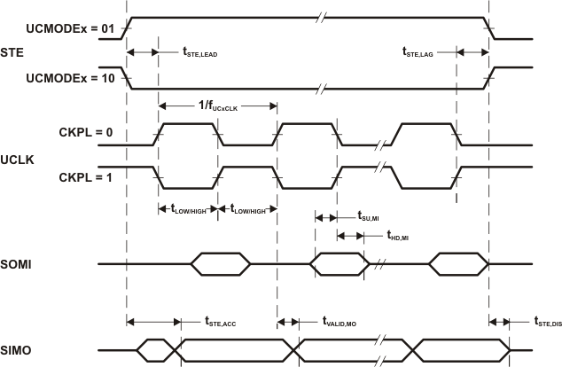 Figure 5-1 SPI Master Mode, CKPH = 0
 Figure 5-2 SPI Master Mode, CKPH = 1
5.14 eUSCI (SPI Slave Mode)
over recommended ranges of supply voltage and operating free-air temperature (unless otherwise noted)(1)| PARAMETER | TEST CONDITIONS | VDDB | MIN | TYP | MAX | UNIT | |
|---|---|---|---|---|---|---|---|
| tSTE,LEAD | STE lead time, STE active to clock | 1.5 V | 7 | ns | |||
| tSTE,LAG | STE lag time, Last clock to STE inactive | 1.5 V | 0 | ns | |||
| tSTE,ACC | STE access time, STE active to SOMI data out | 1.5 V | 65 | ns | |||
| tSTE,DIS | STE disable time, STE inactive to SOMI high impedance | 1.5 V | 40 | ns | |||
| tSU,SI | SIMO input data setup time | 1.5 V | 2 | ns | |||
| tHD,SI | SIMO input data hold time | 1.5 V | 5 | ns | |||
| tVALID,SO | SOMI output data valid time(2) | UCLK edge to SOMI valid, CL = 20 pF |
1.5 V | 30 | ns | ||
| tHD,SO | SOMI output data hold time(3) | CL = 20 pF | 1.5 V | 4 | ns | ||
(1) fUCxCLK = 1/2tLO/HI with tLO/HI ≥ max(tVALID,MO(Master) + tSU,SI(eUSCI), tSU,MI(Master) + tVALID,SO(eUSCI)).
For the master's parameters tSU,MI(Master) and tVALID,MO(Master) see the SPI parameters of the attached slave.
For the master's parameters tSU,MI(Master) and tVALID,MO(Master) see the SPI parameters of the attached slave.
(2) Specifies the time to drive the next valid data to the SOMI output after the output changing UCLK clock edge. See the timing diagrams in Figure 5-3 and Figure 5-4.
(3) Specifies how long data on the SOMI output is valid after the output changing UCLK clock edge. See the timing diagrams in Figure 5-3 and Figure 5-4.
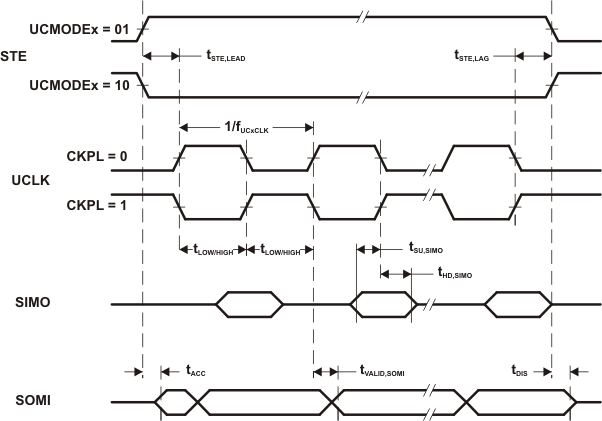 Figure 5-3 SPI Slave Mode, CKPH = 0
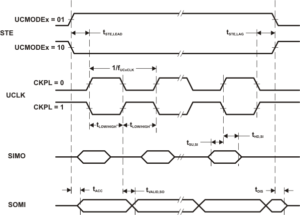 Figure 5-4 SPI Slave Mode, CKPH = 1
5.15 eUSCI (I2C Mode)
over recommended ranges of supply voltage and operating free-air temperature (unless otherwise noted) (see Figure 5-5)| PARAMETER | TEST CONDITIONS | VDDB | MIN | TYP | MAX | UNIT | |
|---|---|---|---|---|---|---|---|
| feUSCI | eUSCI input clock frequency | Internal: SMCLK, ACLK External: UCLK Duty cycle = 50% ± 10% |
fSYSTEM | MHz | |||
| fSCL | SCL clock frequency | 1.5 V | 0 | 400 | kHz | ||
| tHD,STA | Hold time (repeated) START | fSCL = 100 kHz | 1.5 V | 4.0 | µs | ||
| fSCL > 100 kHz | 0.6 | ||||||
| tSU,STA | Setup time for a repeated START | fSCL = 100 kHz | 1.5 V | 4.7 | µs | ||
| fSCL > 100 kHz | 0.6 | ||||||
| tHD,DAT | Data hold time | 1.5 V | 0 | ns | |||
| tSU,DAT | Data setup time | 1.5 V | 250 | ns | |||
| tSU,STO | Setup time for STOP | fSCL = 100 kHz | 1.5 V | 4.0 | µs | ||
| fSCL > 100 kHz | 0.6 | ||||||
| tSP | Pulse duration of spikes suppressed by input filter | UCGLITx = 0 | 1.5 V | 50 | 600 | ns | |
| UCGLITx = 1 | 25 | 300 | ns | ||||
| UCGLITx = 2 | 12.5 | 150 | ns | ||||
| UCGLITx = 3 | 6.25 | 75 | ns | ||||
| tTIMEOUT | Clock low time-out | UCCLTOx = 1 | 1.5 V | 27 | ms | ||
| UCCLTOx = 2 | 30 | ms | |||||
| UCCLTOx = 3 | 33 | ms | |||||
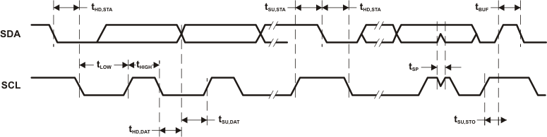 Figure 5-5 I2C Mode Timing
5.16 FRAM
over recommended ranges of supply voltage and operating free-air temperature (unless otherwise noted)| PARAMETER | TEST CONDITIONS | MIN | TYP | MAX | UNIT | |
|---|---|---|---|---|---|---|
| tWRITE | Word or byte write time | 125 | ns | |||
| Read/write endurance | 1015 | cycles | ||||
| tRetention | Data retention duration | TJ = 25°C | 10 | years | ||
5.17 JTAG
over recommended ranges of supply voltage and operating free-air temperature (unless otherwise noted)| PARAMETER | VDDB | MIN | TYP | MAX | UNIT | |
|---|---|---|---|---|---|---|
| fTCK | TCK input frequency, 4-wire JTAG(1) | 1.5 V | 0 | 4 | MHz | |
(1) fTCK may be restricted to meet the timing requirements of the module selected.
5.18 RFPMM, Power Supply Switch
over recommended ranges of supply voltage and operating free-air temperature (unless otherwise noted)| PARAMETER | TEST CONDITIONS | MIN | TYP | MAX | UNIT | |
|---|---|---|---|---|---|---|
| VTH+ | Positive going switching threshold VTH+ = VDDB-VDDR |
35 | 60 | mV | ||
| VTH- | Negative going switching threshold VTH- = VDDB-VDDR |
-60 | -35 | mV | ||
| VHYST | Switching voltage hysteresis VHYST = VTH+-VTH- |
30 | 70 | 110 | mV | |
| IBASVBAT | VDDB input leakage current | VDDB = 1.65 V, Battery switch open | 20 | nA | ||
| VDROP | VDROP= VDDB - VDDSW(1) | 50 | mV | |||
(1) Battery switch closed. Current = 400 µA
5.19 RFPMM, Bandgap Reference
over recommended ranges of supply voltage and operating free-air temperature (unless otherwise noted)| PARAMETER | TEST CONDITIONS | MIN | TYP | MAX | UNIT | |
|---|---|---|---|---|---|---|
| VREF | Output voltage | VDDSW = 1.4 V to 1.65 V | 892 | 908 | mV | |
5.20 RFPMM, Voltage Doubler
over recommended ranges of supply voltage and operating free-air temperature (unless otherwise noted)| PARAMETER | TEST CONDITIONS | MIN | TYP | MAX | UNIT | |
|---|---|---|---|---|---|---|
| VDD2X | Output voltage | VDDSW = 1.4 V, IDD2X = 1 µA, cont = 0 | 2 × VDDSW – 74mV | mV | ||
| VDD2X | Output voltage | VDDSW = 1.4 V, IDD2X = 100 µA, cont = 1 | 2 × VDDSW – 104mV | mV | ||
5.21 RFPMM, Voltage Supervision
over recommended ranges of supply voltage and operating free-air temperature (unless otherwise noted)| PARAMETER | VDDSW | MIN | TYP | MAX | UNIT | |
|---|---|---|---|---|---|---|
| VDDBTH+ | Positive threshold | 1.5 V | 1.45 | V | ||
| VDDBTH- | Negative threshold | 1.5 V | 1.40 | V | ||
| VDDSWTH+ | Positive threshold | 1.40 | V | |||
| VDDSWTH- | Negative threshold | 1.35 | V | |||
| VDDDTH+ | Positive threshold | 1.5 V | 1.00 | V | ||
| VDDDTH- | Negative threshold | 1.5 V | 0.90 | V | ||
| VDD2XTH+ | Positive threshold | 1.5 V | 2.70 | V | ||
| VDD2XTH- | Negative threshold | 1.5 V | 2.475 |
V | ||
5.22 SD14, Performance
over recommended ranges of supply voltage and operating free-air temperature (unless otherwise noted)| PARAMETER | TEST CONDITIONS | MIN | NOM | MAX | UNIT | |
|---|---|---|---|---|---|---|
| fM | Modulator clock frequency | Internal LF oscillator as clock source for SD14 module | 2 | kHz | ||
| RES | Resolution | 8 | 14 | Bit | ||
| OSR | Oversampling ratio | 40 | 2048 | |||
| B | Bandwidth of input signal | 1 | Hz | |||
| VI | Input voltage range | VI = VADCx - VSVSS | 0 | VREF | mV | |
| Voffset | Offset error | Complete signal chain | -0.75 | 0.75 | % of FSR(2) | |
| VGErr | Gain error(1) | complete signal chain | -2% | 2% | ||
| ∆EG/∆T | Gain error temperature coefficient. (3) | complete signal chain | 100 | ppm/K | ||
| EUnadjusted | Total unadjusted error | -2 | 2 | % of FSR(2) | ||
| tStart | Startup time | 20 | CLK cycles | |||
(1) The gain error EG specifies the deviation of the actual gain Gact from the nominal gain Gnom: EG = (Gact – Gnom)/Gnom. It covers process, temperature and supply voltage variations.
(2) FSR = Full Scale Range (SD14 pre-amplifier Gain PGA gain - SD14 gain =1) .
(3) Not production tested.
5.23 SVSS Generator
over recommended ranges of supply voltage and operating free-air temperature (unless otherwise noted)| PARAMETER | TEST CONDITIONS | MIN | TYP | MAX | UNIT | |
|---|---|---|---|---|---|---|
| VSVSS | Output voltage | ISVSS = -5uA .. 0uA | 80 | 125 | 165 | mV |
| tSettling | Settling time after switching SVSS on (95% of final voltage) | Switch from VIRTGND = 1 to VIRTGND = 0 | 400 | 1000 | ms | |
5.24 Thermistor Bias Generator
over recommended ranges of supply voltage and operating free-air temperature (unless otherwise noted)| PARAMETER | TEST CONDITIONS | MIN | TYP | MAX | UNIT | |
|---|---|---|---|---|---|---|
| IOUT,TH | Output current | VOUT = 0 to 0.7 V | 2.0 | 2.4 | 3.0 | µA |
5.25 Temperature Sensor
over recommended ranges of supply voltage and operating free-air temperature (unless otherwise noted)| PARAMETER | TEST CONDITIONS | MIN | TYP | MAX | UNIT | |
|---|---|---|---|---|---|---|
| tc | Temperature coefficient | 35.7 | LSB/K | |||
5.26 RF13M, Power Supply and Recommended Operating Conditions
over recommended ranges of supply voltage and operating free-air temperature (unless otherwise noted)| PARAMETER | TEST CONDITIONS | MIN | TYP | MAX | UNIT | |
|---|---|---|---|---|---|---|
| VDDH | Antenna rectified voltage | IDDH = 100 µA | 1.8 | 2 | 3.6 | V |
| CIN | Input capacitance | 2 V RMS | 31.5 | 35 | 38.5 | pF |
5.27 RF13M, ISO/IEC 15693 ASK Demodulator
over recommended ranges of supply voltage and operating free-air temperature (unless otherwise noted)| PARAMETER | MIN | TYP | MAX | UNIT | |
|---|---|---|---|---|---|
| DR100 | Input signal data rate 100% downlink modulation, 100% ASK, ISO/IEC 15693 | 6 | 26 | kbps | |
| m100 | Modulation depth 100%, test as defined in ISO10373 | 90% | 100% | ||
| m10 | Modulation depth 10%, test as defined in ISO10373 | 7% | 30% | ||
| |tPLH– tPHL| | Delta propagation delay of RXD_10 to VIN | 0 | 2.35 | µs | |
| tPLH, tPHL | Propagation delay of RXD_10 to VIN | 0 | 7.07 | µs | |
| tpd100 | Propagation delay of RXD_100 | 7.07 | µs | ||
| tD100 | Minimum pulse duration of RxD_100 | 5 | µs | ||
5.28 RF13M, ISO/IEC 15693 Compliant Load Modulator
over recommended ranges of supply voltage and operating free-air temperature (unless otherwise noted)| PARAMETER | MIN | TYP | MAX | UNIT | |
|---|---|---|---|---|---|
| fPICC | Uplink subcarrier modulation frequency | 0.2 | 1 | MHz | |
| VA_MOD | Modulated antenna voltage, VA_unmod = 2,3V | 0.5 | V | ||
| VSUB15 | Uplink modulation subcarrier level, ISO/IEC 15693 | 10 | mV | ||