SNVS903B December 2012 – May 2016 SM74611
PRODUCTION DATA.
- 1 Features
- 2 Applications
- 3 Description
- 4 Revision History
- 5 Pin Configuration and Functions
- 6 Specifications
- 7 Detailed Description
- 8 Application and Implementation
- 9 Power Supply Recommendations
- 10Layout
- 11Device and Documentation Support
- 12Mechanical, Packaging, and Orderable Information
Package Options
Mechanical Data (Package|Pins)
- KTT|3
Thermal pad, mechanical data (Package|Pins)
Orderable Information
1 Features
- Maximum Reverse Voltage (VR) of 30 V
- Operating Forward Current (IF) of up to 15 A
- Low Average Forward Voltage (26 mV at 8 A)
- Less Power Dissipation than Schottky Diode
- Lower Leakage Current than Schottky Diode
- Footprint and Pin-Compatible With Conventional D2PAK Schottky Diode
- Operating Range (TJ) of –40°C to 125°C
2 Applications
- Bypass Diodes for Photovoltaic Panels
- Bypass Diodes for Microinverter and Power Optimizer
3 Description
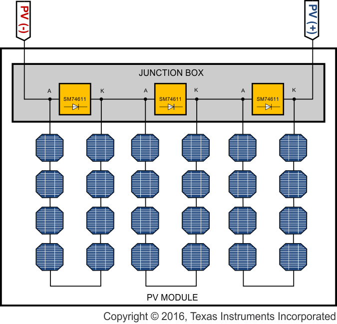
The SM74611 device is a smart bypass diode used in photovoltaic applications. The SM74611 device serves the purpose of providing an alternate path for string current when parts of the panel are shaded during normal operation. Without bypass diodes, the shaded cells will exhibit a hot spot which is caused by excessive power dissipation in the reverse biased cells.
Currently, conventional P-N junction diodes or Schottky diodes are used to mitigate this issue. Unfortunately the forward voltage drop for these diodes is still considered high (approximately 0.6 V for normal diodes and 0.4 V for Schottky). With 10 A of currents flowing through these diodes, the power dissipation can reach as high as 6 W. This in turn will raise the temperature inside the junction box where these diodes normally reside and reduce module reliability.
The advantage of the SM74611 is that it has a lower forward voltage drop than P-N junction and Schottky diodes. It has a typical average forward voltage drop of 26 mV at 8 A of current. This translates into typical power dissipation of 208 mW, which is significantly lower than the 3.2 W of conventional Schottky diodes. The SM74611 is also footprint and pin compatible with conventional D2PAK Schottky diodes, making it a drop-in replacement in many applications.
Device Information(1)
| PART NUMBER | PACKAGE | BODY SIZE (NOM) |
|---|---|---|
| SM74611 | TO-263 (3) | 10.18 mm × 8.41 mm |
- For all available packages, see the orderable addendum at the end of the datasheet.
Typical Application in a Junction Box
