SNVS903B December 2012 – May 2016 SM74611
PRODUCTION DATA.
- 1 Features
- 2 Applications
- 3 Description
- 4 Revision History
- 5 Pin Configuration and Functions
- 6 Specifications
- 7 Detailed Description
- 8 Application and Implementation
- 9 Power Supply Recommendations
- 10Layout
- 11Device and Documentation Support
- 12Mechanical, Packaging, and Orderable Information
Package Options
Mechanical Data (Package|Pins)
- KTT|3
Thermal pad, mechanical data (Package|Pins)
Orderable Information
10 Layout
10.1 Layout Guidelines
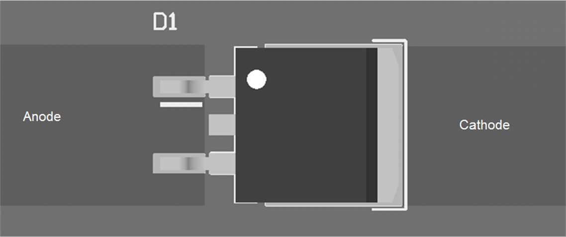
Some layout guidelines must be followed to ensure proper conduction from ANODE to CATHODE pins. ANODE and CATHODE traces carrying the load current must be wide to reduce the amount of parasitic trace inductance as shown in Figure 10.
10.2 Layout Example
 Figure 10. Layout Example for SM74611