SNVS903B December 2012 – May 2016 SM74611
PRODUCTION DATA.
- 1 Features
- 2 Applications
- 3 Description
- 4 Revision History
- 5 Pin Configuration and Functions
- 6 Specifications
- 7 Detailed Description
- 8 Application and Implementation
- 9 Power Supply Recommendations
- 10Layout
- 11Device and Documentation Support
- 12Mechanical, Packaging, and Orderable Information
Package Options
Mechanical Data (Package|Pins)
- KTT|3
Thermal pad, mechanical data (Package|Pins)
Orderable Information
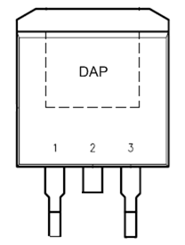
5 Pin Configuration and Functions
KTT Package
3-Pin TO-263
Top View

Pin Functions
| PIN | I/O | DESCRIPTION | |
|---|---|---|---|
| NAME | NO. | ||
| ANODE | 1(1) | I | Connect both of these pins to the negative side of the PV cells |
| 3(1) | |||
| CATHODE | 2(2) | O | Pin 2 and the DAP are shorted internally. Connect the DAP to the positive side of the PV cells |
| DAP(2) | |||
(1) Pin 1 and Pin 3 must be connected together for proper operation.
(2) Package drawing at the end of datasheet is shown without Pin 2 being trimmed.