SGUS034F February 2001 – June 2015 SMJ320VC33
PRODUCTION DATA.
- 1 Features
- 2 Description
- 3 Revision History
- 4 Description (continued)
- 5 Pin Configuration and Functions
-
6 Specifications
- 6.1 Absolute Maximum Ratings
- 6.2 Recommended Operating Conditions
- 6.3 Electrical Characteristics
- 6.4 Phase-Locked Loop Characteristics Using EXTCLK or On-Chip Crystal Oscillator Timing Requirements
- 6.5 Circuit Parameters for On-Chip Crystal Oscillator Timing Requirements
- 6.6 Timing Requirements for EXTCLK, All Modes
- 6.7 Timing Requirements for Memory Read/Write for STRB
- 6.8 Timing Requirements for XF0 and XF1 when Executing LDFI or LDII
- 6.9 Timing Requirements for XF0 and XF1 when Executing SIGI
- 6.10 Timing Requirements for Changing XFx from Output to Input Mode
- 6.11 Timing Requirements for RESET
- 6.12 Timing Requirements for INT3 to INT0 Response
- 6.13 Timing Requirements for Serial Port
- 6.14 Timing Requirements for HOLD/HOLDA
- 6.15 Timing Requirements for Peripheral Pin General-Purpose I/O
- 6.16 Timing Requirements for Timer Pin
- 6.17 Timing Requirements for IEEE-1149.1 Test Access Port
- 6.18 Switching Characteristics for EXTCLK, All Modes
- 6.19 Switching Characteristics for Memory Read/Write for STRB
- 6.20 Switching Characteristics for XF0 and XF1 when Executing LDFI or LDII
- 6.21 Switching Characteristics for XF0 when Executing STFI or STII
- 6.22 Switching Characteristics for XF0 and XF1 when Executing SIGI
- 6.23 Switching Characteristics for Loading when XF is Configured as an Output
- 6.24 Switching Characteristics for Changing XFx from Output to Input Mode
- 6.25 Switching Characteristics for Changing XFx from an Input to an Output
- 6.26 Switching Characteristics for RESET
- 6.27 Switching Characteristics for IACK
- 6.28 Switching Characteristics for Serial Port
- 6.29 Switching Characteristics for HOLD/HOLDA
- 6.30 Switching Characteristics for Peripheral Pin General-Purpose I/O
- 6.31 Switching Characteristics for Timer Pin
- 6.32 Switching Characteristics for SHZ
- 7 Parameter Measurement Information
-
8 Detailed Description
- 8.1 Functional Block Diagram
- 8.2
Feature Description
- 8.2.1 JTAG Scan-Based Emulation Logic
- 8.2.2 Clock Generator
- 8.2.3 PLL and Clock Oscillator Control
- 8.2.4 PLL Isolation
- 8.2.5 Clock and PLL Considerations on Initialization
- 8.2.6 EDGEMODE
- 8.2.7 Reset Operation
- 8.2.8 PAGE0 to PAGE3 Select Lines
- 8.2.9 Using External Logic With the READY Pin
- 8.2.10 Posted Writes
- 8.2.11 Data Bus I/O Buffer
- 8.2.12 Bootloader Operation
- 8.2.13 JTAG Emulation
- 8.2.14 Designing a Target System Emulator Connector (14-Pin Header)
- 8.2.15 JTAG Emulator Cable Pod Logic
- 8.2.16 Reset Timing
- 8.2.17 Interrupt Response TIming
- 8.2.18 Interrupt-Acknowledge Timing
- 8.2.19 Data-Rate Timing Modes
- 8.2.20 HOLD Timing
- 8.2.21 General-Purpose I/O Timing
- 8.2.22 Peripheral Pin I/O Timing
- 8.2.23 Timer Pin Timing
- 8.3 Register Maps
- 9 Power Supply Recommendations
- 10Device and Documentation Support
- 11Mechanical, Packaging, and Orderable Information
Package Options
Refer to the PDF data sheet for device specific package drawings
Mechanical Data (Package|Pins)
- HFG|164
Thermal pad, mechanical data (Package|Pins)
Orderable Information
8 Detailed Description
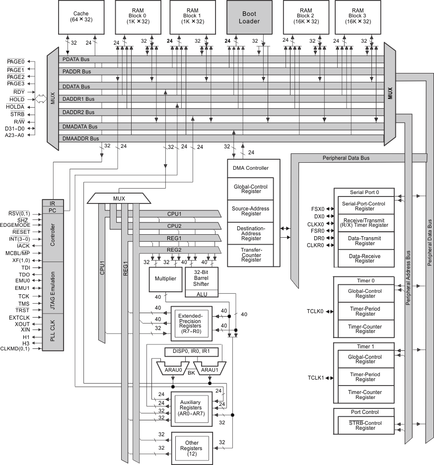
8.1 Functional Block Diagram
8.2 Feature Description
8.2.1 JTAG Scan-Based Emulation Logic
The 320VC33 contains a JTAG port for CPU emulation within a chain of any number of other JTAG devices. The JTAG port on this device does not include a pin-by-pin boundary scan for point-to-point board level test. The Boundary Scan tap input and output is internally connected with a single dummy register allowing loop back tests to be performed through that JTAG domain.
The JTAG emulation port of this device also includes two additional pins, EMU0 and EMU1, for global control of multiple processors conforming to the TI emulation standard. These pins are open collector-type outputs which are wire ORed and tied high with a pullup. Non-TI emulation devices should not be connected to these pins.
The VC33 instruction register is 8 bits long. Table 1 shows the instructions code. The uses of SAMPLE and HIGHZ opcodes, though defined, have no meaning for the SMx320VC33, which has no boundary scan. For example, HIGHZ affects only the dummy cell (no meaning) and does not put the device pins in a high-impedance state.
Table 1. Boundary-Scan Instruction Code
| INSTRUCTION NAME | INSTRUCTION CODE |
|---|---|
| EXTEST | 00000000 |
| BYPASS | 11111111 |
| SAMPLE | 00000010(2) |
| HIGHZ | 00000110(2) |
| PRIVATE1(1) | 00000011 |
| PRIVATE2(1) | 00100000 |
| PRIVATE3(1) | 00100001 |
| PRIVATE4(1) | 00100010 |
| PRIVATE5(1) | 00100011 |
| PRIVATE6(1) | 00100100 |
| PRIVATE7(1) | 00100101 |
| PRIVATE8(1) | 00100110 |
| PRIVATE9(1) | 00100111 |
| PRIVATE10(1) | 00101000 |
| PRIVATE11(1) | 00101001 |
8.2.2 Clock Generator
The clock generator provides clocks to the VC33 device and consists of an internal oscillator and a PLL circuit. The clock generator requires a reference clock input, which can be provided by using a crystal resonator with the internal oscillator, or from an external clock source. The PLL circuit generates the device clock by multiplying the reference clock frequency by a x5 scale factor, allowing use of a clock source with a lower frequency than that of the CPU. The PLL is an adaptive circuit that, once synchronized, locks onto and tracks an input clock signal.
8.2.3 PLL and Clock Oscillator Control
The clock mode control pins are decoded into four operational modes as shown in Figure 25. These modes control clock divide ratios, oscillator, and PLL power (see Table 2).
When an external clock input or crystal is connected, the opposite unused input is simply grounded. An XOR gate then passes one of the two signal sources to the PLL stage. This allows the direct injection of a clock reference into EXTCLK, or 1- to 20-MHz crystals and ceramic resonators with the oscillator circuit. The two clock sources include:
- A crystal oscillator circuit, where a crystal or ceramic resonator is connected across the XOUT and XIN pins and EXTCLK is grounded.
- An external clock input, where an external clock source is directly connected to the EXTCLK pin, and XOUT is left unconnected and XIN is grounded.
When the PLL is initially started, it enters a transitional mode during which the PLL acquires lock with the input signal. When the PLL is locked, it continues to track and maintain synchronization with the input signal. The PLL is a simple ×5 reference multiplier with bypass and power control.
The clock divider, under CPU control, reduces the clock reference by 1 (MAXSPEED), 1/16 (LOWPOWER), or clock stop (IDLE2). Wake-up from the IDLE2 state is accomplished by a RESET or interrupt pin logic-low state.
A divide-by-two TMS320C31 equivalent mode of operation is also provided. In this case, the clock output reference is further divided by two with clock synchronization being determined by the timing of RESET falling relative to the present H1/H3 state.
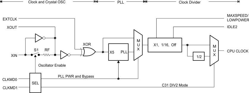 Figure 25. Clock Generation
Table 2. Clock Mode Select Pins
| CLKMD0 | CLKMD1 | FEEDBACK | PLLPWR | RATIO | NOTES |
|---|---|---|---|---|---|
| 0 | 0 | Off | Off | 1 | Fully static, very-low power |
| 0 | 1 | On | Off | 1/2 | Oscillator enabled |
| 1 | 0 | On | Off | 1 | Oscillator enabled |
| 1 | 1 | On | On | 5 | 2 mA at 60 MHz, 1.8-V PLL power. Oscillator enabled |
Typical crystals in the 8- to 30-MHz range have a series resistance of 25 Ω, which increases below 8 MHz. To maintain proper filtering and phase relationships, Rd and Zout of the oscillator circuit should be 10x to 40x that of the crystal. TI recommends a series compensation resistor (Rd), shown in Figure 26, when using lower frequency crystals. The XOUT output, the square wave inverse of XIN, is then filtered by the XOUT output impedance, C1 load capacitor, and Rd (if present). The crystal and C2 input load capacitor then refilters this signal, resulting in a XIN signal that is 75% to 85% of the oscillator supply voltage.
NOTE
Some ceramic resonators are available in a low-cost, three-pin package that includes C1 and C2 internally. Typically, ceramic resonators do not provide the frequency accuracy of crystals.
Better PLL stability can be achieved using the optional power supply isolation circuit shown in Figure 26. A similar filter can be used to isolate the PLLVSS, as shown in Figure 27. PLLVDD can also be directly connected to CVDD.
Table 3. Typical Crystal Circuit Loading
| FREQUENCY (MHz) | Rd (Ω) | C1 (pF) | C2 (pF) | CL(1) (pF) | RL(1) (Ω) |
|---|---|---|---|---|---|
| 2 | 4.7k | 18 | 18 | 12 | 200 |
| 5 | 2.2k | 18 | 18 | 12 | 60 |
| 10 | 470 | 15 | 15 | 12 | 30 |
| 15 | 0 | 15 | 12 | 12 | 25 |
| 20 | 0 | 9 | 9 | 10 | 25 |
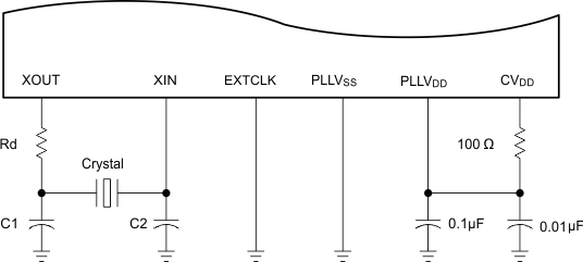 Figure 26. Self-Oscillation Mode
8.2.4 PLL Isolation
The internal PLL supplies can be directly connected to CVDD and VSS (0-Ω case), partially isolated as shown in Figure 26, or fully isolated as shown in Figure 27. The RC network prevents the PLL supplies from turning high-frequency noise in the CVDD and VSS supplies into jitter.
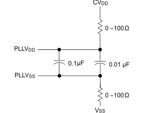 Figure 27. PLL Isolation Circuit Diagram
8.2.5 Clock and PLL Considerations on Initialization
On power up, the CPU clock divide mode can be in MAXSPEED, LOPOWER, or IDLE2, or the PLL could be in an undefined mode. RESET falling in the presence of a valid CPU clock is used to clear this state, after which the device will synchronously terminate any external activity.
The 5× Fclkin PLL of the 320VC33 contains an 8-bit PLL–LOCK counter that causes the PLL to output a frequency of Fclkin / 2 during the initial ramp. However, this counter does not increment while RESET is low or in the absence of an input clock. A minimum of 256 input clocks are required before the first falling edge of reset for the PLL to output to clear this counter. The following describes the setup and behavior that is observed. Power is applied to the DSP with RESET low and the input clock high or low. A clock is applied (RESET is still low) and the PLL appears to lock onto the input clock, producing the expected ×5 output frequency. RESET is driven high and the PLL output immediately drops to Fclkin / 2 for up to 256 input cycles or 128 of the Fclkin / 2 output cycles. The PLL/CPU clock then switches to ×5 mode.
The switch over is synchronous and does not create a clock glitch, so the only effect is that the CPU runs slow for up to the first 128 cycles after reset goes high. After the PLL has stabilized, the counter remains cleared and subsequent resets do not exhibit this condition.
Systems that are not using the crystal oscillator may be required to supply a current of 250 mA per DSP if full power is applied with no clock source. This extra current condition is a result of uninitialized internal logic within the DSP core and is corrected when the CPU sees a minimum of four internal clocks. The crystal oscillator is typically immune to this condition since the oscilator and core circuitry become semi-functional at CVDD = 1 V where the fault current is considerably lower. An alternate clock pulse can also be applied to either the EXTCLK or XIN clock input pins.
8.2.6 EDGEMODE
When EDGEMODE = 1, a sampled digital delay line is decoded to generate a pulse on the falling edge of the interrupt pin. To ensure interrupt recognition, input signal logic-high and logic-low states must be held longer than the synchronizer delay of one CPU clock cycle. Holding these inputs to no less than two cycles in both the logic-low and logic-high states is sufficient.
When EDGEMODE = 0, a logic-low interrupt pin continually sets the corresponding interrupt flag. The CPU or DMA can clear this flag within two cycles of it being set. This is the maximum interrupt width that can be applied if only one interrupt is to be recognized. The CPU can manually clear IF bits within an interrupt service routine (ISR), effectively lengthening the maximum ISR width.
After reset, EDGEMODE is temporarily disabled, allowing logic-low INT pins to be detected for bootload operation.
 Figure 28. EDGEMODE and Interrupt Flag Circuit
8.2.7 Reset Operation
When RESET is applied, the CPU attempts to safely exit any pending read or write operations that may be in progress. This can take as much as 10 CPU cycles, after which, the address, data, and control pins are in an inactive or high-impedance state.
When both RESET and SHZ are applied, the device immediately enters the reset state with the pins held in high-impedance mode. SHZ should then be disabled at least 10 CPU cycles before RESET is set high. SHZ can be used during power-up sequencing to prevent undefined address, data, and control pins, avoiding system conflicts.
8.2.8 PAGE0 to PAGE3 Select Lines
To facilitate simpler and higher-speed connection to external devices, the SMx320VC33 includes four predecoded select pins that have the same timings as STRB.These pins are decoded from A22, A23, and STRB and are active only during external accesses over the ranges shown in Table 4. A single bus control register controls all external bus accesses.
Table 4. PAGE0 to PAGE3 Ranges
| START | END | |
|---|---|---|
| PAGE0 | 0x000000 | 0x3FFFFF |
| PAGE1 | 0x400000 | 0x7FFFFF |
| PAGE2 | 0x800000 | 0xBFFFFF |
| PAGE3 | 0xC00000 | 0xFFFFFF |
8.2.9 Using External Logic With the READY Pin
The key to designing external wait-state logic is the internal bus control register and associated internal logic that logically combines the external READY pin with the much faster on-chip bus control logic. This essentially allows slow external logic to interact with the bus while easily meeting the READY input timings. Note that the combined ready signals are sampled on the rising edge of the internal H1 clock. Refer to Figure 29 for the following examples.
Example 1: A simple 0 or WTCNT wait-state decoder can be created by simply tying an address line back to the READY pin and selecting the AND option. When the tied back address is low, the bus runs with 0 wait states. When the tied back address is high, the bus is controlled by the internal wait-state counter.
By enabling the bank compare logic, proper operation is further ensured by inserting a null cycle before a read on the next bank is performed (writes are not pre-extended). This extra time can also be used by external logic to affect the feedback path.
Example 2: An N–WTCNT minimum wait-state decoder can also be created by tying back an address line to READY and logically ORing it with the internal bank compare and wait count signals. When the address pin is low, bus timing is determined by the internal WTCNT and BNKCMP settings. When the address line is high, the bus can run no faster than the WTCNT counter and is extended as long as READY is held high.
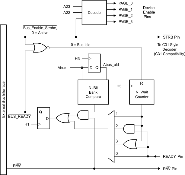 Figure 29. Internal Ready Logic, Simplified Diagram
Table 5. MUX Select (Bus Control Register Bits 4 and 3)
| BIT 4 | BIT 3 | RESULTS |
|---|---|---|
| 0 | 0 | Ignore internal wait counter and use only external READY |
| 0 | 1 | Use only internal wait counter and ignore ready pin |
| 1 | 0 | Logical AND internal wait counter with ready pin |
| 1 | 1 | Logical OR internal wait counter with ready pin (reset default) |
8.2.10 Posted Writes
External writes are effectively “posted” to the bus, which then acts like an output latch until the write completes. Therefore, if the application code is executing internally, it can perform a very-slow external write with no penalty because the bus acts like it has a one-level-deep write FIFO.
8.2.11 Data Bus I/O Buffer
The circuit shown in Figure 30 is incorporated into each data pin to lightly “hold” the last driven value on the data bus pins when the DSP or an external device is not actively driving the bus. Each bus keeper is built from a three-state driver with nominal 15-kΩ output resistance which is fed back to the input in a positive feedback configuration. The resistance-isolated driver then pulls the output in one direction or the other keeping the last driven value. This circuit is enabled in all functional modes and is only disabled when SHZ is pulled low.
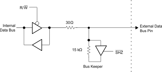 Figure 30. Bus Keeper Circuit
For an external device to change the state of these pins, it must be able to drive a small dc current until the driver threshold is crossed. At the crossover point, the driver changes state, agreeing with the external driver and assisting the change. The voltage threshold of the bus keeper is approximately at 50% of the DVDD supply voltage. The typical output impedance of 30 Ω for all SMx320VC33 I/O pins is easily capable of meeting this requirement.
8.2.12 Bootloader Operation
When MCBL/MP = 1, an internal ROM is decoded into the address range of 0x000000 to 0x000FFF. Therefore, when reset occurs, execution begins within the internal ROM program and vector space. No external activity is evident until one of the boot options is enabled. These options are enabled by pulling an external interrupt pin low, which the boot-load software then detects, causing a particular routine to be executed (see Table 6).
Table 6. INT0 to INT3 Sources
| ACTIVE INTERRUPT | ADDRESS/SOURCE WHERE BOOT DATA IS READ FROM | DATA FORMAT |
|---|---|---|
| INT0 | 0x001000 | 8-, 16-, or 32-bit width |
| INT1 | 0x400000 | 8-, 16-, or 32-bit width |
| INT2 | 0xFFF000 | 8-, 16-, or 32-bit width |
| INT3 | Serial port | 32-bit, external clock, and frame synch |
When MCBL/MP = 1, the reset and interrupt vectors are hard-coded within the internal ROM. Because this is a read-only device, these vectors cannot be modified. To enable user-defined interrupt routines, the internal vectors contain fixed values that point to an internal section of SRAM beginning at 0x809FC1. Code execution begins at these locations, so it is important to place branch instructions (to the interrupt routine) at these locations and not vectors.
The bootloader program requires a small stack space for calls and returns. Two SRAM locations at 0x809800 and 0x809801 are used for this stack. Do not boot load data into these locations because it will corrupt the bootloader program runtime stack. After the boot-load operation is complete, a program can reclaim these locations. The simplest solution is to begin a program stack or uninitialized data section at 0x809800.
For additional details on bootloader operation including the bootloader source code, see the TMS320C3x User’s Guide (SPRU031).
A bit I/O line or external logic can be used to safely disable the MCBL mode after bootloading is complete. However, to ensure proper operation, the CPU should not be currently executing code or using external data as the change takes place. In the following example, the XF0 pin is tri-state on reset, which allows the pullup resistor to place the DSP in MCBL mode. The following code, placed at the beginning of an application then causes the XF0 pin to become an active-logic-low output, changing the DSP mode to MP. The cache-enable and RPTS instructions are used because they cause the LDI instruction to be executed multiple times even though it has been fetched only once (before the mode change). In other words, the RPTS instruction acts as a one-level-deep program cache for externally executed code. If the application code is to be executed from internal RAM, no special provisions are needed.
LDI    8000h,ST ; Enable the cache
RPTS   4        ; RPTS will fetch the following opcode 1 time
LDI    2h, IOF  ; Drive MCBL/MP=0 for several cycles allowing
                ; the pipeline to clear
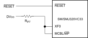 Figure 31. Changing Bootload Select Pin
8.2.13 JTAG Emulation
Though the 320VC33 contains a JTAG debug port which allows multiple JTAG enabled chips to be daisy-chained, boundary scan of the pins is not supported. If the pin scan path is selected, it will be routed through a null register with a length of one. For additional information concerning the emulation interface, see JTAG/MPSD Emulation Technical Reference (SPDU079).
8.2.14 Designing a Target System Emulator Connector (14-Pin Header)
JTAG target devices support emulation through a dedicated emulation port. This port is a superset of the test access port standard and is accessed by the emulator. To communicate with the emulator, the target system must have a 14-pin header (two rows of seven pins) with the connections that are shown in Figure 32. Table 7 describes the emulation signals.
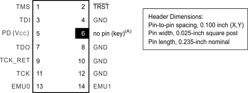
Table 7. 14-Pin Header Signal Descriptions
| SIGNAL | DESCRIPTION | EMULATOR(1) STATE | TARGET(1) STATE |
|---|---|---|---|
| TMS(2) | Test mode select | O | I |
| TDI | Test data input | O | I |
| TDO | Test data output | I | O |
| TCK | Test clock. TCK is a 10.368-MHz clock source from the emulation cable pod. This signal can be used to drive the system test clock | O | I |
| TRST(3) | Test reset | O | I |
| EMU0(2)(4) | Emulation pin 0 | I | I/O |
| EMU1(2)(4) | Emulation pin 1 | I | I/O |
| PD(VCC) | Presence detect. Indicates that the emulation cable is connected and that the target is powered up. PD should be tied to VCC in the target system. | I | O |
| TCK_RET | Test clock return. Test clock input to the emulator. May be a buffered or unbuffered version of TCK. | I | O |
| GND | Ground | — | — |
Although other headers can be used, recommended parts include: straight header, unshrouded DuPont™ connector systems part numbers:
- 65610–114
- 65611–114
- 67996–114
- 67997–114
8.2.15 JTAG Emulator Cable Pod Logic
Figure 33 shows a portion of the emulator cable pod. The functional features of the pod are as follows:
- Signals TDO and TCK_RET can be parallel-terminated inside the pod if required by the application. By default, these signals are not terminated.
- Signal TCK is driven with a 74LVT240 device. Because of the high-current drive (32 mA IOL/IOH), this signal can be parallel-terminated. If TCK is tied to TCK_RET, the parallel terminator in the pod can be used.
- Signals TMS and TDI can be generated from the falling edge of TCK_RET, according to the bus slave device timing rules.
- Signals TMS and TDI are series-terminated to reduce signal reflections.
- A 10.368-MHz test clock source is provided. Another test clock can be used for greater flexibility.
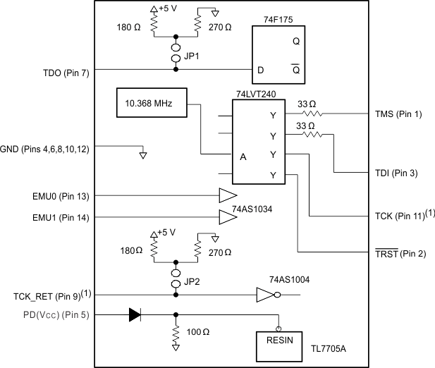
- The emulator pod uses TCK_RET as its clock source for internal synchronization. TCK is provided as an optional target system test clock source.
8.2.16 Reset Timing
RESET is an asynchronous input that can be asserted at any time during a clock cycle. If the specified timings are met, the exact sequence shown in Figure 14 occurs; otherwise, an additional delay of one clock cycle is possible.
The asynchronous reset signals include XF0/1, CLKX0, DX0, FSX0, CLKR0, DR0, FSR0, and TCLK0/1.
Resetting the device initializes the bus control register to seven software wait states and therefore results in slow external accesses until these registers are initialized.
HOLD is a synchronous input that can be asserted during reset. It can take nine CPU cycles before HOLDA is granted.
Timing Requirements for RESET defines the timing parameters for the RESET signal.
8.2.17 Interrupt Response TIming
The interrupt (INTx) pins are synchronized inputs that can be asserted at any time during a clock cycle. The TMS320C3x interrupts are selectable as level- or edge-sensitive. Interrupts are detected on the falling edge of H1. Therefore, interrupts must be set up and held to the falling edge of the internal H1 for proper detection. The CPU and DMA respond to detected interrupts on instruction-fetch boundaries only.
For the processor to recognize only one interrupt when level mode is selected, an interrupt pulse must be set up and held such that a logic-low condition occurs for:
- A minimum of one H1 falling edge
- No more than two H1 falling edges
- Interrupt sources whose edges cannot be specified to meet the H1 falling edge setup and hold times must be further restricted in pulse width as defined by tw(INT) in Timing Requirements for INT3 to INT0 Response.
When EDGEMODE = 1, the falling edge of the INT0 to INT3 pins are detected using synchronous logic (see Figure 28). The pulse low and high time should be two CPU clocks or greater.
The TMS320C3x can set the interrupt flag from the same source as quickly as two H1 clock cycles after it has been cleared.
If the specified timings are met, the exact sequence shown in Figure 15 occurs; otherwise, an additional delay of one clock cycle is possible.
8.2.18 Interrupt-Acknowledge Timing
The IACK output goes active on the first half-cycle (HI rising) of the decode phase of the IACK instruction and goes inactive at the first half-cycle (HI rising) of the read phase of the IACK instruction.
Switching Characteristics for IACK defines the timing parameters for the IACK signal.
NOTE
The IACK instruction can be executed at anytime to signal an event. It is most often used within an interrupt routine to signal which interrupt has occurred. The IACK instruction must be executed to generate the IACK pulse.
8.2.19 Data-Rate Timing Modes
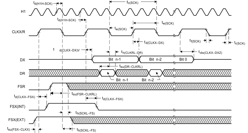
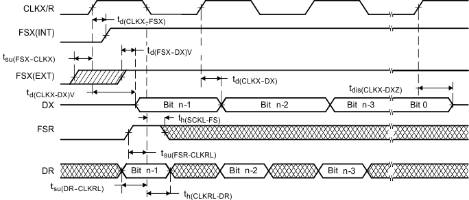
Unless otherwise indicated, the data-rate timings shown in Figure 34 and Figure 35 are valid for all serial-port modes, including handshake. For a functional description of serial-port operation, see the TMS320C3x User’s Guide (SPRU031).
The serial-port timing parameters are defined in Timing Requirements for Serial Port.
8.2.20 HOLD Timing
HOLD is a synchronous input that can be asserted at any time during a clock cycle. If the specified timings are met, the exact sequence shown in Figure 17 and Figure 18 occurs; otherwise, an additional delay of one clock cycle is possible.
Timing Requirements for HOLD/HOLDA defines the timing parameters for the HOLD and HOLDA signals.
The NOHOLD bit of the primary-bus control register overrides the HOLD signal. When this bit is set, the device comes out of hold and prevents future hold cycles.
Asserting HOLD prevents the processor from accessing the primary bus. Program execution continues until a read from or a write to the primary bus is requested. In certain circumstances, the first write is pending, thus allowing the processor to continue (internally) until a second external write is encountered.
Figure 17, Figure 18, and the accompanying timings are for a zero wait-state bus configuration. Because HOLD is internally captured by the CPU on the H1 falling edge one cycle before the present cycle is terminated, the minimum HOLD width for any bus configuration is, therefore, WTCNT + 3. Also, do not deassert HOLD before HOLDA has been active for at least one cycle.
8.2.21 General-Purpose I/O Timing
Peripheral pins include CLKX0, CLKR0, DX0, DR0, FSX0, FSR0, and TCLK0/1. The contents of the internal control registers associated with each peripheral define the modes for these pins.
8.2.22 Peripheral Pin I/O Timing
Timing Requirements for Peripheral Pin General-Purpose I/O shows the timing parameters for changing the peripheral pin from a general-purpose output pin to a general-purpose input pin and vice versa.
8.2.23 Timer Pin Timing
Valid logic-level periods and polarity are specified by the contents of the internal control registers.
8.3 Register Maps
NOTE:
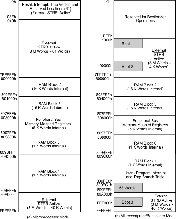
STRB is active over all external memory ranges. PAGE0 to PAGE3 are configured as external bus strobes. These are simple decoded strobes that have no configuration registers and are active only during external bus activity over the following ranges:Table 8. SMx320VC33 Memory Map Active Ranges
| Name | Active Range |
|---|---|
| PAGE0 | 0000000h – 03FFFFFh |
| PAGE1 | 0400000h – 07FFFFFh |
| PAGE2 | 0800000h – 0BFFFFFh |
| PAGE3 | 0C00000h – 0FFFFFFh |
| STRB | 0000000h – 0FFFFFFh |
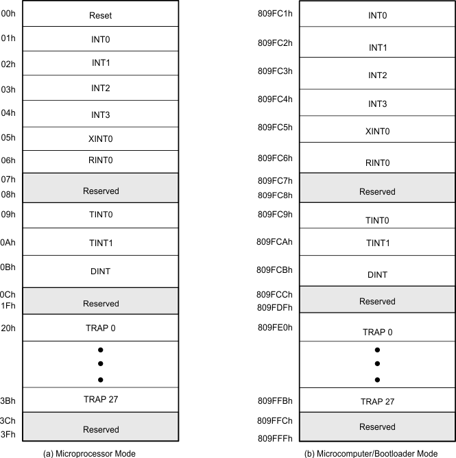 Figure 37. Reset, Interrupt, and Trap Vector/Branches Memory-Map Locations
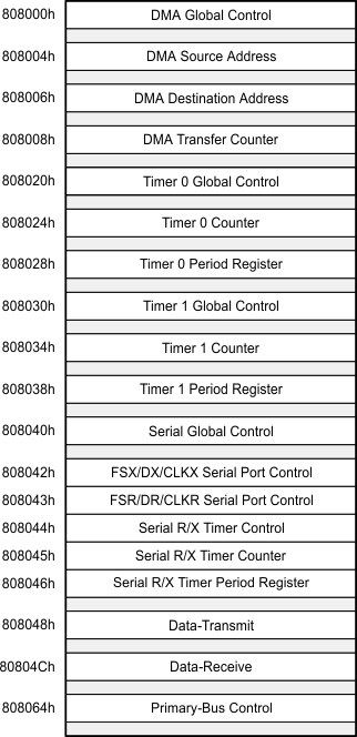
NOTE:
Shading denotes reserved address locations.