SDLS049C December 1983 – November 2016 SN5414 , SN54LS14 , SN7414 , SN74LS14
PRODUCTION DATA.
- 1 Features
- 2 Applications
- 3 Description
- 4 Revision History
- 5 Pin Configuration and Functions
- 6 Specifications
- 7 Parameter Measurement Information
- 8 Detailed Description
- 9 Application and Implementation
- 10Power Supply Recommendations
- 11Layout
- 12Device and Documentation Support
- 13Mechanical, Packaging, and Orderable Information
Package Options
Refer to the PDF data sheet for device specific package drawings
Mechanical Data (Package|Pins)
- J|14
- W|14
Thermal pad, mechanical data (Package|Pins)
Orderable Information
7 Parameter Measurement Information
7.1 Series SN5414 and SN7414 Devices
 Figure 14. Load Circuit For
2-State Totem-Pole Outputs
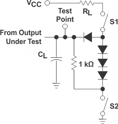 Figure 16. Load Circuit For 3-State Outputs
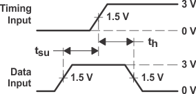 Figure 18. Voltage Waveforms
Setup and Hold Times
 Figure 15. Load Circuit For
Open-Collector Outputs
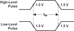 Figure 17. Voltage Waveforms Pulse Durations
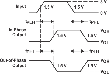 Figure 19. Voltage Waveforms
Propagation Delay Times
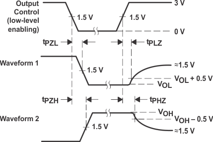
A. CL includes probe and jig capacitance.
B. All diodes are 1N3064 or equivalent.
C. Waveform 1 is for an output with internal conditions such that the output is low except when disabled by the output control. Waveform 2 is for an output with internal conditions such that the output is high except when disabled by the output control.
D. S1 and S2 are closed for tPLH, tPHL, tPHZ, and tPLZ; S1 is open and S2 is closed for tPZH; S1 is closed and S2 is open for tPZL.
E. All input pulses are supplied by generators having the following characteristics: PRR ≤ 1 MHz, ZO ≈ 50 Ω ; tr and tf ≤ 7 ns for Series SN5414 and SN7414 devices and tr and tf ≤ 2.5 ns for Series SN54S14 and SN74S14 devices.
F. The outputs are measured one at a time with one input transition per measurement.
Figure 20. Voltage Waveforms Enable and Disable Times, 3-State Outputs
7.2 Series SN54LS14 and SN74LS14 Devices
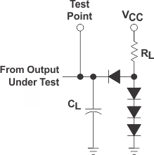 Figure 21. Load Circuit For
2-State Totem-Pole Outputs
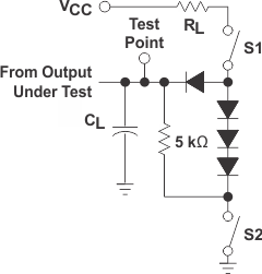 Figure 23. Load Circuit For 3-State Outputs
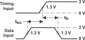 Figure 25. Voltage Waveforms
Setup and Hold Times
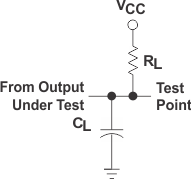 Figure 22. Load Circuit For
Open-Collector Outputs
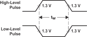 Figure 24. Voltage Waveforms Pulse Durations
 Figure 26. Voltage Waveforms
Propagation Delay Times
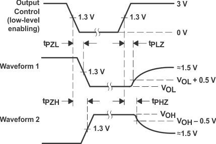
A. CL includes probe and jig capacitance.
B. All diodes are 1N3064 or equivalent.
C. Waveform 1 is for an output with internal conditions such that the output is low except when disabled by the output control. Waveform 2 is for an output with internal conditions such that the output is high except when disabled by the output control.
D. S1 and S2 are closed for tPLH, tPHL, tPHZ, and tPLZ; S1 is open and S2 is closed for tPZH; S1 is closed and S2 is open for tPZL.
E. Phase relationships between inputs and outputs have been chosen arbitrarily for these examples.
F. All input pulses are supplied by generators having the following characteristics: PRR ≤ 1 MHz, ZO ≈ 50 Ω, tr ≤ 1.5 ns, tf ≤ 2.6 ns.
G. The outputs are measured one at a time with one input transition per measurement.
Figure 27. Voltage Waveforms Enable and Disable Times, 3-State Outputs