SCHS367C October 2008 – April 2022 SN54AC00-SP
PRODUCTION DATA
- 1Features
- 2Applications
- 3Description
- 4Revision History
- 5Bare Die Information
- 6Specifications
- 7Parameter Measurement Information
- 8Device and Documentation Support
- 9Mechanical, Packaging, and Orderable Information
Package Options
Mechanical Data (Package|Pins)
Thermal pad, mechanical data (Package|Pins)
Orderable Information
5 Bare Die Information
| DIE THICKNESS | BACKSIDE FINISH | BACKSIDE POTENTIAL | BOND PAD METALLIZATION COMPOSITION |
BOND PAD THICKNESS |
|---|---|---|---|---|
| 15 mils | Silicon with backgrind | Floating | TiW/AlCu2 | 15800 nm |
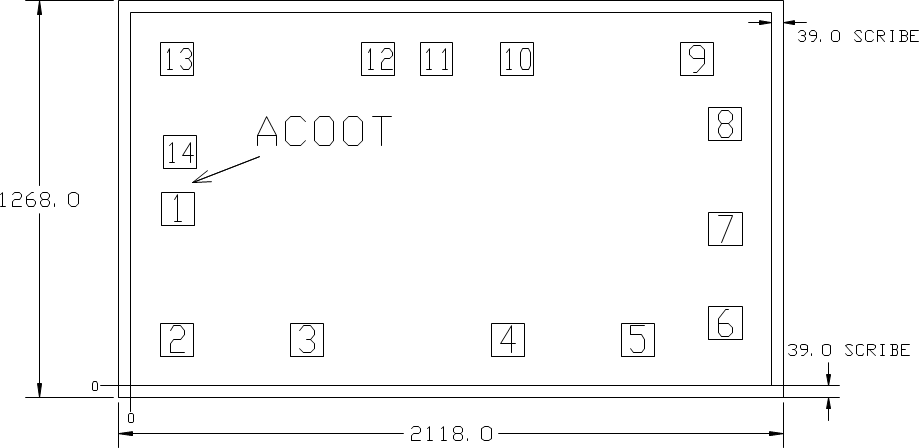
Bond Pad Coordinates in Microns
| DESCRIPTION | PAD NUMBER | X MIN | Y MIN | X MAX | Y MAX |
|---|---|---|---|---|---|
| 1A | 1 | 96.3 | 510.5 | 201.3 | 615.5 |
| 1B | 2 | 95 | 94 | 200 | 199 |
| 1Y | 3 | 508 | 94 | 613 | 199 |
| 2A | 4 | 1149 | 94 | 1254 | 199 |
| 2B | 5 | 1562 | 94 | 1667 | 199 |
| 2Y | 6 | 1841.5 | 145.5 | 1946.5 | 250.5 |
| GND | 7 | 1841.5 | 445.5 | 1946.5 | 550.5 |
| 3Y | 8 | 1841 | 783 | 1946 | 888 |
| 3A | 9 | 1750.5 | 991 | 1855.5 | 1096 |
| 3B | 10 | 1176.5 | 991 | 1281.5 | 1096 |
| 4Y | 11 | 921 | 991 | 1026 | 1096 |
| 4A | 12 | 736 | 991 | 841 | 1096 |
| 4B | 13 | 95 | 991 | 200 | 1096 |
| VCC | 14 | 102.5 | 692 | 207.5 | 797 |