SCLS231P october 1995 – june 2023 SN54AHC04 , SN74AHC04
PRODMIX
- 1
- 1Features
- 2Description
- 3Revision History
- 4Pin Configuration and Functions
- 5Specifications
- 6Parameter Measurement Information
- 7Detailed Description
- 8Device and Documentation Support
- 9Mechanical, Packaging, and Orderable Information
Package Options
Refer to the PDF data sheet for device specific package drawings
Mechanical Data (Package|Pins)
- J|14
- FK|20
- W|14
Thermal pad, mechanical data (Package|Pins)
Orderable Information
4 Pin Configuration and Functions
 |
 |
 |
|
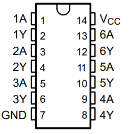
Figure 4-1 SN54AHC04 J or W Package SN74AHC04 D, DB, DGV, N,
NS, or PW Package (Top View)
|
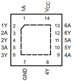
Figure 4-2 SN74AHC04 RGY or BQA Package (Top View)
|
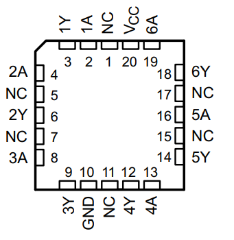
Figure 4-3 SN54AHC04 FK Package (Top View)
|
Table 4-1 Pin Functions
| PIN | I/O | DESCRIPTION | |||||
|---|---|---|---|---|---|---|---|
| NAME | SN74AHC04 | SN54AHC04 | |||||
| D, DB, DGV, N, NS, PW |
RGY, BQA | J, W | FK | ||||
| 1A | 1 | 1 | 1 | 2 | I | 1A Input | |
| 1Y | 2 | 2 | 2 | 3 | O | 1Y Output | |
| 2A | 3 | 3 | 3 | 4 | I | 2A Input | |
| 2Y | 4 | 4 | 4 | 6 | O | 2Y Output | |
| 3A | 5 | 5 | 5 | 8 | I | 3A Input | |
| 3Y | 6 | 6 | 6 | 9 | O | 3Y Output | |
| 4A | 9 | 9 | 9 | 13 | I | 4A Input | |
| 4Y | 8 | 8 | 8 | 12 | O | 4Y Output | |
| 5A | 11 | 11 | 11 | 16 | I | 5A Input | |
| 5Y | 10 | 10 | 10 | 14 | I | 5Y Output | |
| 6A | 13 | 13 | 13 | 19 | I | 6A Input | |
| 6Y | 12 | 12 | 12 | 18 | O | 6Y Output | |
| GND | 7 | 7 | 7 | 10 | — | Ground Pin | |
| NC | — | — | — | 1 | — | No Connection | |
| 5 | |||||||
| 7 | |||||||
| 11 | |||||||
| 15 | |||||||
| 17 | |||||||
| VCC | 14 | 14 | 14 | 20 | — | Power Pin | |