SCLS005E March 1984 – February 2022 SN54HCT374 , SN74HCT374
PRODUCTION DATA
- 1 Features
- 2 Description
- 3 Revision History
- 4 Pin Configuration and Functions
- 5 Specifications
- 6 Parameter Measurement Information
- 7 Detailed Description
- 8 Power Supply Recommendations
- 9 Layout
- 10Device and Documentation Support
- 11Mechanical, Packaging, and Orderable Information
Package Options
Refer to the PDF data sheet for device specific package drawings
Mechanical Data (Package|Pins)
- J|20
- FK|20
Thermal pad, mechanical data (Package|Pins)
Orderable Information
2 Description
These 8-bit flip-flops feature 3-state outputs designed specifically for driving highly capacitive or relatively low-impedance loads. They are particularly suitable for implementing buffer registers, I/O ports, bidirectional bus drivers, and working registers.
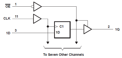
The eight flip-flops of the ’HCT374 devices are edge-triggered D-type flip-flops. On the positive transition ofthe clock (CLK) input, the Q outputs are set to the logic levels that were set up at the data (D) inputs.
An output-enable (OE) input places the eight outputs in either a normal logic state (high or low logic levels) or the high-impedance state. In the high-impedance state, the outputs neither load nor drive the bus lines significantly. The high-impedance state and increased drive provide the capability to drive bus lines without interface or pullup components.
| PART NUMBER | PACKAGE(1) | BODY SIZE (NOM) |
|---|---|---|
| SN74HCT374DW | SOIC (20) | 12.80 mm × 7.50 mm |
| SN74HCT374DB | SSOP (20) | 7.20 mm × 5.30 mm |
| SN74HCT374N | PDIP (20) | 25.40 mm × 6.35 mm |
| SN74HCT374NS | SO (20) | 15.00 mm × 5.30 mm |
| SN74HCT374PW | TSSOP (20) | 6.50 mm × 4.40 mm |
| SN54HCT374J | CDIP (20) | 26.92 mm × 6.92 mm |
| SNJ54HCT374FK | LCCC (20) | 8.89 mm × 8.45 mm |
 Functional Block
Diagram