SDLS144D April 1985 – October 2016 SN54LS240 , SN54LS241 , SN54LS244 , SN54S240 , SN54S241 , SN54S244 , SN74LS240 , SN74LS241 , SN74LS244 , SN74S240 , SN74S241 , SN74S244
- 1 Features
- 2 Applications
- 3 Description
- 4 Revision History
- 5 Pin Configuration and Functions
-
6 Specifications
- 6.1 Absolute Maximum Ratings
- 6.2 ESD Ratings
- 6.3 Recommended Operating Conditions
- 6.4 Thermal Information
- 6.5 Electrical Characteristics - SNx4LS24x
- 6.6 Electrical Characteristics - SNx4S24x
- 6.7 Switching Characteristics - SNx4LS24x
- 6.8 Switching Characteristics - SNx4S24x
- 6.9 Typical Characteristics
- 7 Parameter Measurement Information
- 8 Detailed Description
- 9 Application and Implementation
- 10Power Supply Recommendations
- 11Layout
- 12Device and Documentation Support
- 13Mechanical, Packaging, and Orderable Information
Package Options
Mechanical Data (Package|Pins)
Thermal pad, mechanical data (Package|Pins)
Orderable Information
9 Application and Implementation
NOTE
Information in the following applications sections is not part of the TI component specification, and TI does not warrant its accuracy or completeness. TI’s customers are responsible for determining suitability of components for their purposes. Customers should validate and test their design implementation to confirm system functionality.
9.1 Application Information
The SNx4LS24x, SNx4S24x octal buffers and line drivers are designed to be used for a multitude of bus interface type applications where output drive or PCB trace length is a concern.
9.2 Typical Application
 Figure 22. SNx4LS241 and SNx4S241 Used as Repeater or Level Restorer
9.2.1 Design Requirements
This device uses Schottky transistor logic technology. Take care to avoid bus contention because it can drive currents that would exceed maximum limits. The high drive creates fast edges into light loads, so routing and load conditions must be considered to prevent ringing.
9.2.2 Detailed Design Procedure
- Power Supply
- Each device must maintain a supply voltage between 4.5 V and 5.5 V.
- Inputs
- Input signals must meet the VIH and VIL specifications in Electrical Characteristics – SNx4LS24x.
- Inputs leakage values (II, IIH, IIL) from Electrical Characteristics – SNx4LS24x must be considered.
- Outputs
- Output signals are specified to meet the VOH and VOL specifications in Electrical Characteristics – SNx4LS24x as a minimum (the values could be closer to VCC for high signals or GND for low signals).
- TI recommends maintaining output currents as specified in Recommended Operating Conditions.
- The part can be damaged by sourcing or sinking too much current (see Electrical Characteristics – SNx4LS24x for details).
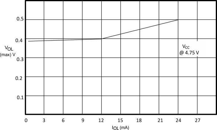
9.2.3 Application Curve
 Figure 23. VOL vs IOL
9.3 System Examples
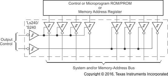
The SNx4LS240 and SNx4S240 devices can be used to buffer signals along a memory bus. The increased output drive helps data transmission reliability. Figure 24 shows a schematic of this example.

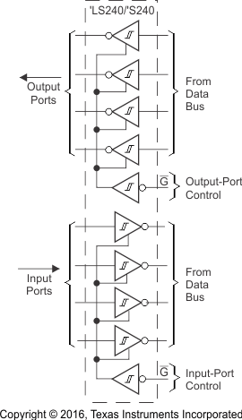
The SNx4LS240 and SNx4S240 devices have two independently controlled 4-bit drivers, and can be used to buffer signals in a bidirectional manner along a data bus. Figure 25 shows the SNx4LS240 or SNx4S240 used in this manner.
 Figure 25. Independent 4-Bit But Drivers/Receivers in a Single Package
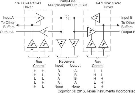
The enable pins on the SNx4LS241 and SNx4S241 devices can be used to help direct signals along a shared party-line bus. Figure 26 shows a general configuration of how to implement this structure. Take care to ensure that bus contention does not occur.
 Figure 26. Party-Line Bus System With Multiple Inputs, Outputs, and Receivers