SLLS266J February 1997 – August 2022 SN65220 , SN65240 , SN75240
PRODUCTION DATA
- 1 Features
- 2 Applications
- 3 Description
- 4 Revision History
- 5 Device Comparison Table
- 6 Pin Configuration and Functions
- 7 Specifications
- 8 Parameter Measurement Information
- 9 Detailed Description
- 10Application and Implementation
- 11Power Supply Recommendations
- 12Layout
- 13Device and Documentation Support
- 14Mechanical, Packaging, and Orderable Information
Package Options
Mechanical Data (Package|Pins)
- DBV|6
Thermal pad, mechanical data (Package|Pins)
Orderable Information
3 Description
The SN65220 device is a dual, and the SN65240 and SN75240 devices are quadruple, unidirectional transient voltage suppressors (TVS). These devices provide electrical noise transient protection to Universal Serial Bus (USB) low and full-speed ports. The input capacitance of 35 pF makes it unsuitable for high-speed USB 2.0 applications.
Any cabled I/O can be subjected to electrical noise transients from various sources. These noise transients can cause damage to the USB transceiver or the USB ASIC if they are of sufficient magnitude and duration.
The SN65220, SN65240, and SN75240 devices ESD performance is measured at the system level, according to IEC61000-4-2; system design, however, impacts the results of these tests. To accomplish a high compliance level, careful board design and layout techniques are required.
| PART NUMBER | PACKAGE | BODY SIZE (NOM) |
|---|---|---|
| SN65220 | SOT-23 (6) | 2.90 mm × 1.60 mm |
| DSBGA (4) | 0.925 mm × 0.925 mm | |
| SN65240 SN75240 |
PDIP (8) | 9.09 mm × 6.35 mm |
| TSSOP (8) | 3.00 mm × 4.40 mm |
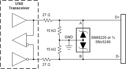
 Simplified Schematic
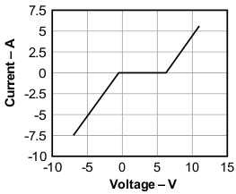
 TVS Current vs
Voltage