SLLSES6C February 2016 – December 2021 SN65DP141
PRODUCTION DATA
- 1 Features
- 2 Applications
- 3 Description
- 4 Revision History
- 5 Pin Configuration and Functions
- 6 Specifications
- 7 Parameter Measurement Information
-
8 Detailed Description
- 8.1 Overview
- 8.2 Functional Block Diagram
- 8.3 Feature Description
- 8.4 Device Functional Modes
- 8.5
Register Maps
- 8.5.1 Register 0x00 (General Device Settings) (offset = 00000000) [reset = 00000000]
- 8.5.2 Register 0x01 (Channel Enable) (offset = 00000000) [reset = 00000000]
- 8.5.3 Register 0x02 (Channel 0 Control Settings) (offset = 00000000) [reset = 00000000]
- 8.5.4 Register 0x03 (Channel 0 Enable Settings) (offset = 00000000) [reset = 00000000]
- 8.5.5 Register 0x05 (Channel 1 Control Settings) (offset = 00000000) [reset = 00000000]
- 8.5.6 Register 0x06 (Channel 1 Enable Settings) (offset = 00000000) [reset = 00000000]
- 8.5.7 Register 0x08 (Channel 2 Control Settings) (offset = 00000000) [reset = 00000000]
- 8.5.8 Register 0x09 (Channel 2 Enable Settings) (offset = 00000000) [reset = 00000000]
- 8.5.9 Register 0x0B (Channel 3 Control Settings) (offset = 00000000) [reset = 00000000]
- 8.5.10 Register 0x0C (Channel 3 Control Settings) (offset = 00000000) [reset = 00000000]
- 9 Application and Implementation
- 10Power Supply Recommendations
- 11Layout
- 12Device and Documentation Support
- 13Mechanical, Packaging, and Orderable Information
Package Options
Mechanical Data (Package|Pins)
- RLJ|38
Thermal pad, mechanical data (Package|Pins)
Orderable Information
9.2.2 Detailed Design Procedure
Designing in the SN65DP141 requires the following:
- Determine the loss profile on the DP input and output channels and cables.
- Based upon the loss profile and signal swing, determine the optimal configuration for the SN65DP141, to pass electrical compliance (Equalization mode, EQ Gain, DC gain, and AC Gain).
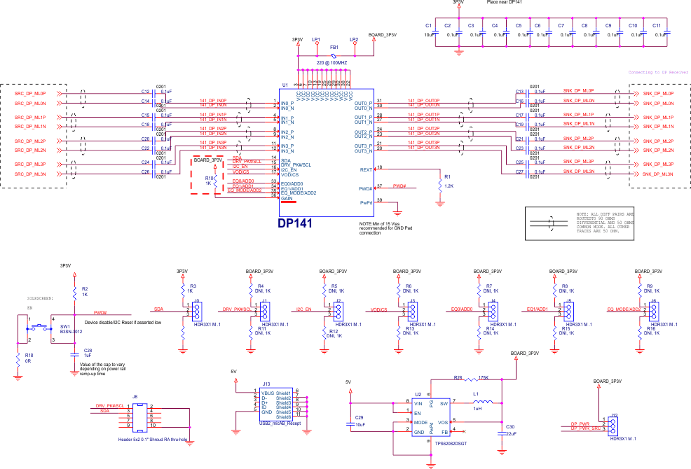
- See Figure 9-2 for information on using the AC coupling capacitors and control pin resistors, as well as for recommended decouple capacitors from VCC pins to ground.
- Configure the TheSN65DP141 using the GPIO terminals or the I2C interface:
- GPIO – Using the terminals EQ_MODE, EQ1, EQ1, and gain.
- I2C – Refer to the I2C Register Maps and the Two-Wire Serial Interface and Control Logic sections for a detailed configuration procedures.
- The thermal pad must be connected to ground.
 Figure 9-2 SN65DP141 Application Schematic