SLLS926B December 2008 – November 2014 SN65EPT22
PRODUCTION DATA.
- 1Features
- 2Applications
- 3Description
- 4Simplified Schematic
- 5Revision History
- 6Pin Configuration and Functions
- 7Specifications
- 8Device and Documentation Support
- 9Mechanical, Packaging, and Orderable Information
Package Options
Mechanical Data (Package|Pins)
Thermal pad, mechanical data (Package|Pins)
Orderable Information
7 Specifications
7.1 Absolute Maximum Ratings(1)
| PARAMETER | CONDITION | MIN | MAX | UNIT |
|---|---|---|---|---|
| Absolute supply voltage, VCC | 6 | V | ||
| Absolute input voltage, VI | GND = 0 and VI ≤ VCC | 0 | 6 | V |
| Supply voltage LVPEL | 3.3 | V | ||
| Output current | Continuous | 50 | mA | |
| Surge | 100 | |||
| Operating temperature range | –40 | 85 | °C | |
(1) Stresses beyond those listed under absolute maximum ratings may cause permanent damage to the device. These are stress ratings only, and functional operation of the device at these or any other conditions beyond those indicated under recommended operating conditions is not implied. Exposure to absolute-maximum-rated conditions for extended periods may affect device reliability.
7.2 Handling Ratings
| MIN | MAX | UNIT | |||
|---|---|---|---|---|---|
| Tstg | Storage temperature range | –65 | 150 | °C | |
| V(ESD) | Electrostatic discharge | Human body model (HBM), per ANSI/ESDA/JEDEC JS-001, all pins(1) | –4 | 4 | kV |
| Charged device model (CDM), per JEDEC specification JESD22-C101, all pins(2) | –2 | 2 | |||
(1) JEDEC document JEP155 states that 500-V HBM allows safe manufacturing with a standard ESD control process.
(2) JEDEC document JEP157 states that 250-V CDM allows safe manufacturing with a standard ESD control process.
7.3 Power Dissipation Ratings
| PACKAGE | CIRCUIT BOARD MODEL | POWER RATING TA < 25°C (mW) |
THERMAL RESISTANCE, JUNCTION TO AMBIENT NO AIRFLOW |
DERATING FACTOR TA > 25°C (mW/°C) |
POWER RATING TA = 85°C (mW) |
|---|---|---|---|---|---|
| D | Low-K | 719 | 139 | 7 | 288 |
| High-K | 840 | 119 | 8 | 336 | |
| DGK | Low-K | 469 | 213 | 5 | 188 |
| High-K | 527 | 189 | 5 | 211 |
7.4 Thermal Information
| THERMAL METRIC(1) | D | DGK | UNIT | |
|---|---|---|---|---|
| 8 PINS | 8 PINS | |||
| RθJB | Junction-to-board thermal resistance | 79 | 120 | °C/W |
| RθJC | Junction-to-case thermal resistance | 98 | 74 | |
(1) For more information about traditional and new thermal metrics, see the IC Package Thermal Metrics application report, SPRA953.
7.5 Key Attributes
| CHARACTERISTICS | VALUE |
|---|---|
| Moisture sensitivity level | Lead free package |
| SOIC-8 | Level 1 |
| VSSOP-8 | Level 3 |
| Flammability rating (Oxygen Index: 28 to 34) | UL 94 V-0 at 0.125 in |
| Meets or exceeds JEDEC Spec EIA/JESD78 latchup test | |
7.6 TTL Input DC Characteristics(1)
(VCC = 3.3 V, GND = 0, TA = –40°C to 85°C)| CHARACTERISTIC | CONDITION | MIN | TYP | MAX | UNIT | |
|---|---|---|---|---|---|---|
| IIH | Input HIGH current | VIN = 2.7 V | 20 | μA | ||
| IIHH | Input HIGH current max | VIN = VCC | 100 | μA | ||
| IIL | Input LOW current | VIN = 0.5 V | –0.6 | mA | ||
| VIK | Input clamp voltage | IIN = –18 mA | –1 | V | ||
| VIH | Input high voltage | 2.0 | V | |||
| VIL | Input low voltage | 0.8 | V | |||
(1) Device will meet the specifications after thermal balance has been established when mounted in a socket or printed circuit board with maintained transverse airflow greater than 500 lfpm. Electrical parameters are assured only over the declared operating temperature range. Functional operation of the device exceeding these conditions is not implied. Device specification limit values are applied individually under normal operating conditions and not valid simultaneously.
7.7 PECL Output DC Characteristics(1)
(VCC = 3.3 V; GND = 0.0V) (2)| CHARACTERISTIC | –40°C | 25°C | 85°C | UNIT | |||||||
|---|---|---|---|---|---|---|---|---|---|---|---|
| MIN | TYP | MAX | MIN | TYP | MAX | MIN | TYP | MAX | |||
| ICC | Power supply current | 39 | 45 | 42 | 47 | 45 | 50 | mA | |||
| VOH | Output HIGH voltage (3) | 2155 | 2224 | 2405 | 2155 | 2224 | 2405 | 2155 | 2224 | 2405 | mV |
| VOL | Output LOW voltage(3) | 1355 | 1441 | 1605 | 1355 | 1438 | 1605 | 1355 | 1435 | 1605 | mV |
(1) Device will meet the specifications after thermal balance has been established when mounted in a socket or printed circuit board with maintained transverse airflow greater than 500 lfpm. Electrical parameters are assured only over the declared operating temperature range. Functional operation of the device exceeding these conditions is not implied. Device specification limit values are applied individually under normal operating conditions and not valid simultaneously.
(2) Output parameters vary 1:1 with VCC
(3) All loading with 50Ω to VCC –2.0V
7.8 AC Characteristics (1)
(VCC = 3.0 V to 3.6 V; GND = 0 V)(2)| CHARACTERISTIC | –40°C | 25°C | 85°C | UNIT | |||||||
|---|---|---|---|---|---|---|---|---|---|---|---|
| MIN | TYP | MAX | MIN | TYP | MAX | MIN | TYP | MAX | |||
| fMAX | Max switching frequency(5), see Figure 5 | 2.1 | 2.0 | 2.0 | GHz | ||||||
| tPLH / tPHL | Propagation delay to differential output | 230 | 550 | 230 | 550 | 230 | 550 | ps | |||
| tSKEW | Within device skew(3) | 25 | 50 | 25 | 50 | 25 | 50 | ps | |||
| Device to device skew(4) | 100 | 200 | 100 | 200 | 100 | 200 | ps | ||||
| tJITTER | Random clock jitter (RMS) | 0.2 | 0.8 | 0.2 | 0.8 | 0.2 | 0.8 | ps | |||
| tr / tf | Output rise/fall times (20%–80%) | 150 | 300 | 150 | 300 | 150 | 300 | ps | |||
(1) Device will meet the specifications after thermal equilibrium has been established when mounted in a test socket or printed circuit board with maintained transverse airflow greater than 500 lfpm. Electrical parameters are assured only over the declared operating temperature range. Functional operation of the device exceeding these conditions is not implied. Device specification limit values are applied individually under normal operating conditions and not valid simultaneously.
(2) Measured using a 2.4 V source, 50% duty cycle clock source. All loading with 50 Ω to VCC – 2.0 V.
(3) Skew is measured between outputs under identical transitions and conditions on any one device.
(4) Device−to−Device Skew for identical transitions at identical VCC levels.
(5) Maximum switching frequency measured at output amplitude of 300 mVpp.
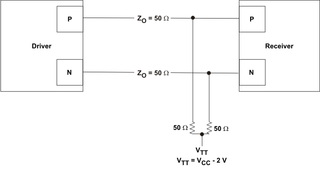 Figure 1. Termination for Output Driver
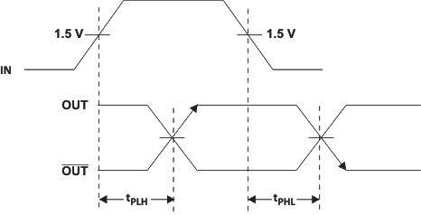 Figure 2. Output Propagation Delay
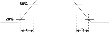 Figure 3. Output Rise and Fall Times
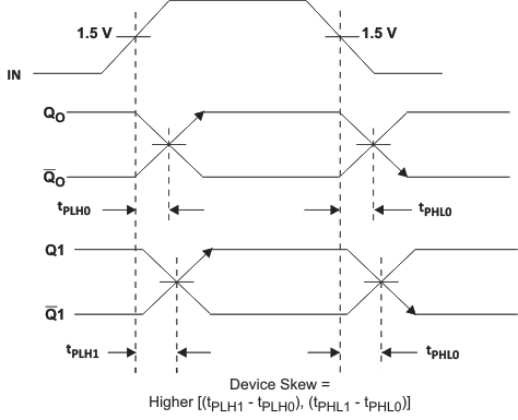 Figure 4. Device Skew
7.9 Typical Characteristics
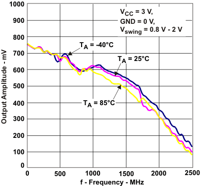 Figure 5. Output Amplitude versus Frequency