SLLS505P February 2002 – February 2022 SN65HVD10 , SN65HVD11 , SN65HVD12 , SN75HVD12
PRODUCTION DATA
- 1 Features
- 2 Applications
- 3 Description
- 4 Revision History
- 5 Device Comparison Table
- 6 Pin Configuration and Functions
-
7 Specifications
- 7.1 Absolute Maximum Ratings
- 7.2 ESD Ratings
- 7.3 Recommended Operating Conditions
- 7.4 Thermal Information
- 7.5 Driver Electrical Characteristics
- 7.6 Receiver Electrical Characteristics
- 7.7 Power Dissipation Characteristics
- 7.8 Driver Switching Characteristics
- 7.9 Receiver Switching Characteristics
- 7.10 Dissipation Ratings
- 7.11 Typical Characteristics
- 8 Parameter Measurement Information
- 9 Detailed Description
- 10Application and Implementation
- 11Power Supply Recommendations
- 12Layout
- 13Device and Documentation Support
- 14Mechanical, Packaging, and Orderable Information
Package Options
Mechanical Data (Package|Pins)
Thermal pad, mechanical data (Package|Pins)
Orderable Information
8 Parameter Measurement Information
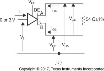 Figure 8-1 Driver
VOD Test Circuit and Voltage and Current Definitions
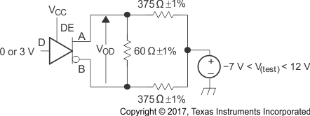 Figure 8-2 Driver
VOD With Common-Mode Loading Test Circuit
Input: PRR = 500
kHz, 50% Duty Cycle, tr < 60 ns, tf < 6 ns
ZO = 50 Ω
Figure 8-3 Test
Circuit and Definitions for the Driver Common-Mode Output Voltage
Generator: PRR =
500 kHz, 50% Duty Cycle, tr < 60 ns, tf < 6 ns
ZO = 50 Ω
Figure 8-4 Driver
Switching Test Circuit and Voltage Waveforms
Generator: PRR =
500 kHz, 50% Duty Cycle, tr < 60 ns, tf < 6 ns
ZO = 50 Ω
Figure 8-5 Driver
High-Level Enable and Disable Time Test Circuit and Voltage Waveforms
Generator: PRR =
500 kHz, 50% Duty Cycle, tr < 60 ns, tf < 6 ns
ZO = 50 Ω
Figure 8-6 Driver
Low-Level Output Enable and Disable Time Test Circuit and Voltage
Waveforms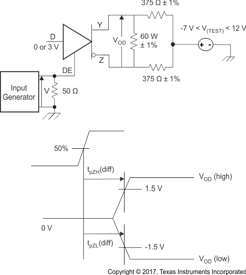
The time
tPZL(x) is the measure from DE to VOD(x).
VOD is valid when it is greater than 1.5 V.
Figure 8-7 Driver
Enable Time from DE to VOD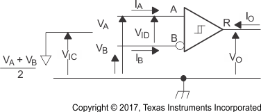 Figure 8-8 Receiver
Voltage and Current Definitions
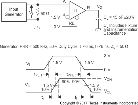 Figure 8-9 Receiver
Switching Test Circuit and Voltage Waveforms
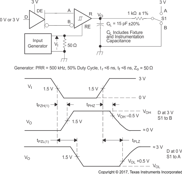 Figure 8-10 Receiver
Enable and Disable Time Test Circuit and Voltage Waveforms With Drivers
Enabled
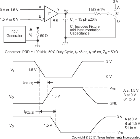 Figure 8-11 Receiver
Enable Time From Standby (Driver Disabled)
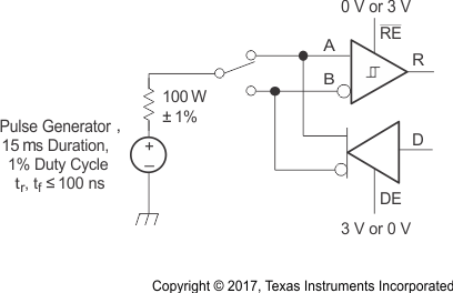
NOTE: This test is
conducted to test survivability only. Data stability at the R output is not
specified.
Figure 8-12 Test
Circuit, Transient Over Voltage Test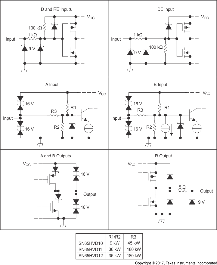 Figure 8-13 Equivalent Input and Output
Schematic Diagrams