SLLSEJ8E June 2014 – April 2019 SN65HVD1470 , SN65HVD1471 , SN65HVD1473 , SN65HVD1474 , SN65HVD1476 , SN65HVD1477
PRODUCTION DATA.
- 1 Features
- 2 Applications
- 3 Description
- 4 Revision History
- 5 Device Comparison Table
- 6 Pin Configuration and Functions
-
7 Specifications
- 7.1 Absolute Maximum Ratings
- 7.2 ESD Ratings
- 7.3 Recommended Operating Conditions
- 7.4 Thermal Information — D Packages
- 7.5 Thermal Information — DGS and DGK Packages
- 7.6 Power Dissipation
- 7.7 Electrical Characteristics
- 7.8 Switching Characteristics — 400 kbps
- 7.9 Switching Characteristics — 20 Mbps
- 7.10 Switching Characteristics — 50 Mbps
- 7.11 Typical Characteristics
- 8 Parameter Measurement Information
- 9 Detailed Description
- 10Application and Implementation
- 11Power Supply Recommendations
- 12Layout
- 13Device and Documentation Support
- 14Mechanical, Packaging, and Orderable Information
Package Options
Mechanical Data (Package|Pins)
Thermal pad, mechanical data (Package|Pins)
Orderable Information
10.2 Typical Application
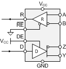
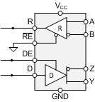
A full-duplex RS-485 network consists of multiple transceivers connecting in parallel to two bus cables. On one signal pair, a master driver transmits data to multiple slave receivers. The master driver and slave receivers may remain fully enabled at all times. On the other signal pair, multiple slave drivers transmit data to the master receiver. To avoid bus contention, the slave drivers must be intermittently enabled and disabled such that only one driver is enabled at any time, as in half-duplex communication. The master receiver may remain fully enabled at all times.
Because the driver may not be disabled, only one driver should be connected to the bus when using the SN65HVD1471, SN65HVD1474, or SN65HVD1477 device.
Master Enable Control

Slave Enable Control
