SLLSEA2D December 2011 – May 2015 SN65HVD255 , SN65HVD256 , SN65HVD257
PRODUCTION DATA.
- 1 Features
- 2 Applications
- 3 Description
- 4 Revision History
- 5 Device Options
- 6 Pin Configuration and Functions
- 7 Specifications
- 8 Parameter Measurement Information
- 9 Detailed Description
- 10Application and Implementation
- 11Power Supply Recommendations
- 12Layout
- 13Device and Documentation Support
- 14Mechanical, Packaging, and Orderable Information
Package Options
Mechanical Data (Package|Pins)
- D|8
Thermal pad, mechanical data (Package|Pins)
Orderable Information
1 Features
- Meets the Requirements of ISO11898-2
- Turbo CAN:
- Short and Symmetrical Propagation Delay Times and Fast Loop Times for Enhanced Timing Margin
- Higher Data Rates in CAN Networks
- I/O Voltage Range Supports 3.3-V and 5-V MCUs
- Ideal Passive Behavior When Unpowered
- Bus and Logic Pins are High Impedance (No Load)
- Power Up and Power Down With Glitch-Free Operation on Bus
- Protection Features
- HBM ESD Protection Exceeds ±12 kV
- Bus Fault Protection –27 V to 40 V
- Undervoltage Protection on Supply Pins
- Driver Dominant Time Out (TXD DTO)
- SN65HVD257: Receiver-Dominant Time Out (RXD DTO)
- SN65HVD257: FAULT Output Pin
- Thermal Shutdown Protection
- Characterized for –40°C to 125°C Operation
2 Applications
- 1-Mbps Operation in Highly Loaded CAN Networks Down to 10-kbps Networks Using TXD DTO
- Industrial Automation, Control, Sensors, and Drive Systems
- Building, Security, and Climate Control Automation
- Telecom Base Station Status and Control
- SN65HVD257: Functional Safety With Redundant and Multitopology CAN networks
- CAN Bus Standards Such as CANopen, DeviceNet, NMEA2000, ARNIC825, ISO11783, and CANaerospace
3 Description
This CAN transceiver meets the ISO1189-2 High Speed CAN (Controller Area Network) Physical Layer standard. It is designed for data rates in excess of
1 Mbps for CAN in short networks, and enhanced timing margin and higher data rates in long and highly-loaded networks. The device provides many protection features to enhance device and CAN-network robustness. The SN65HVD257 device adds additional features, allowing for easy design of redundant and multitopology networks with fault indication for higher levels of functional safety in the CAN system.
Device Information(1)
| PART NUMBER | PACKAGE | BODY SIZE (NOM) |
|---|---|---|
| SN65HVD255 SN65HVD256 SN65HVD257 |
SOIC (8) | 4.90 mm × 3.91 mm |
- For all available packages, see the orderable addendum at the end of the data sheet.
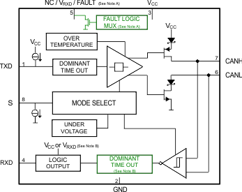
Block Diagram

A. Pin 5 function is device dependent; NC on the SN65HVD255 device, VRXD for RXD output level-shifting device on the SN65HVD256 device, and FAULT Output on the SN65HVD257 device.
B. RXD logic output is driven to 5-V VCC on
5-V only supply devices (SN65HVD255, SN65HVD257) and driven to VRXD on the output level-shifting device (SN65HVD256).
5-V only supply devices (SN65HVD255, SN65HVD257) and driven to VRXD on the output level-shifting device (SN65HVD256).
C. RXD (Receiver) Dominant State Time Out is a device-dependent option available only on the SN65HVD257 device.