SLLSEI3A September 2013 – November 2015 SN65HVD265 , SN65HVD266 , SN65HVD267
PRODUCTION DATA.
- 1 Features
- 2 Applications
- 3 Description
- 4 Revision History
- 5 Device Comparison Table
- 6 Pin Configurations and Functions
- 7 Specifications
- 8 Parameter Measurement Information
- 9 Detailed Description
- 10Application and Implementation
- 11Power Supply Recommendations
- 12Layout
- 13Device and Documentation Support
- 14Mechanical, Packaging, and Orderable Information
Package Options
Mechanical Data (Package|Pins)
- D|8
Thermal pad, mechanical data (Package|Pins)
Orderable Information
9 Detailed Description
9.1 Overview
This CAN transceiver meets the ISO1189-2 High Speed CAN (Controller Area Network) physical layer standard. It is designed for data rates in excess of 2 Mpbs (megabits per second) for CAN FD (CAN with flexible data rate), greater than 1 Mbps for CAN in short networks, and enhanced timing margin and higher data rates in long and highly-loaded networks. The device provides many protection features to enhance device and CAN-network robustness. The SN65HVD267 adds additional features, allowing easy design of redundant and multi-topology networks with fault indication for higher levels of safety in the CAN system.
9.2 Functional Block Diagram
9.3 Feature Description
9.3.1 TXD Dominant Timeout (DTO)
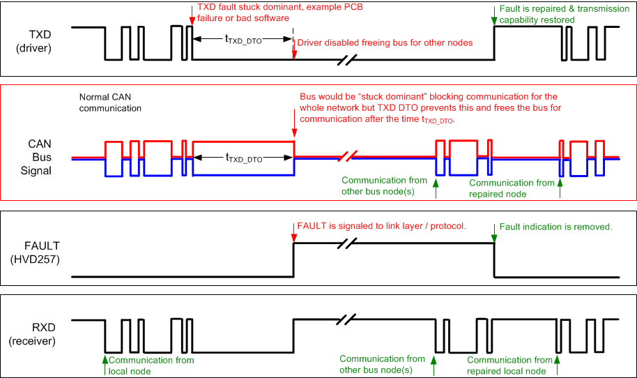
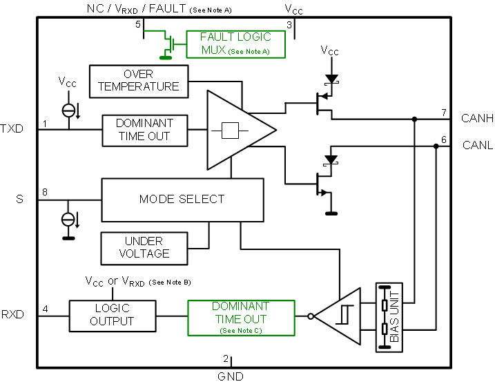
During normal mode (the only mode where the CAN driver is active), the TXD DTO circuit prevents the transceiver from blocking network communication in the event of a hardware or software failure where TXD is held dominant longer than the timeout period tTXD_DTO. The DTO circuit timer starts on a falling edge on TXD. The DTO circuit disables the CAN bus driver if no rising edge is seen before the timeout period expires. This frees the bus for communication between other nodes on the network. The CAN driver is re-activated when a recessive signal is seen on TXD terminal, thus clearing the TXD DTO condition. The receiver and RXD terminal still reflect the CAN bus, and the bus terminals are biased to recessive level during a TXD dominant timeout.
NOTE
The minimum dominant TXD time allowed by the TXD DTO circuit limits the minimum possible transmitted data rate of the device. The CAN protocol allows a maximum of eleven successive dominant bits (on TXD) for the worst case, where five successive dominant bits are followed immediately by an error frame. This, along with the tTXD_DTO minimum, limits the minimum data rate. Calculate the minimum transmitted data rate by: Minimum Data Rate = 11 / tTXD_DTO.
9.3.1.1 RXD Dominant Timeout (SN65HVD267)
The SN65HVD267 device has a RXD dominant timeout (RXD DTO) circuit that prevents a bus stuck dominant fault from permanently driving the RXD output dominant (low) when the bus is held dominant longer than the timeout period tRXD_DTO. The RXD DTO timer starts on a falling edge on RXD (bus going dominant). If no rising edge (bus returning recessive) is seen before the timeout constant of the circuit expires (tRXD_DTO), the RXD terminal returns high (recessive). The RXD output is re-activated to mirror the bus receiver output when a recessive signal is seen on the bus, clearing the RXD dominant timeout. The CAN bus terminals are biased to the recessive level during a RXD DTO.
NOTE
APPLICATION NOTE: The minimum dominant RXD time allowed by the RXD DTO limits the minimum possible received data rate of the device. The CAN protocol allows a maximum of eleven successive dominant bits for the worst case transmission, where five successive dominant bits are followed immediately by an error frame. This, along with the tRXD_DTO minimum, limits the minimum data rate. The minimum received data rate may be calculated by: Minimum Data Rate = 11 / tRXD_DTO.
9.3.1.2 Thermal Shutdown
If the junction temperature of the device exceeds the thermal shut down threshold the device turns off the CAN driver circuits thus blocking the TXD to bus transmission path. The shutdown condition is cleared when the junction temperature drops below the thermal shutdown temperature of the device.
NOTE
During thermal shutdown the CAN bus drivers turn off; thus no transmission is possible from TXD to the bus. The CAN bus terminals are biased to recessive level during a thermal shutdown, and the receiver to RXD path remains operational.
9.3.1.3 Undervoltage Lockout
The supply terminals have undervoltage detection that places the device in protected mode. This protects the bus during an undervoltage event on either the VCC or VRXD supply terminals.
Table 2. Undervoltage Lockout 5-V Only Devices (SN65HVD265 and SN65HVD267)
| VCC | DEVICE STATE | BUS OUTPUT | RXD |
|---|---|---|---|
| GOOD | Normal | Per Device State and TXD | Mirrors Bus |
| BAD | Protected | High Impedance | High Impedance (3-state) |
Table 3. Undervoltage Lockout 5-V and VRXD Device (SN65HVD266)
| VCC | VRXD | DEVICE STATE | BUS OUTPUT | RXD |
|---|---|---|---|---|
| GOOD | GOOD | Normal | Per Device State and TXD | Mirrors Bus |
| BAD | GOOD | Protected | High Impedance | High (Recessive) |
| GOOD | BAD | Protected | Recessive | High Impedance (3-state) |
| BAD | BAD | Protected | High Impedance | High Impedance (3-state) |
NOTE
After an undervoltage condition is cleared and the supplies have returned to valid levels, the device typically resumes normal operation in 300 µs.
9.3.1.4 Fault Terminal (SN65HVD267)
If one or more of the faults (TXD-Dominant Timeout, RXD dominant Timeout, Thermal Shutdown or Undervoltage Lockout) occurs, the FAULT terminal (open-drain) turns off, resulting in a high level when externally pulled up to VCC or IO supply.
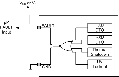 Figure 11. FAULT Terminal Function Diagram and Application
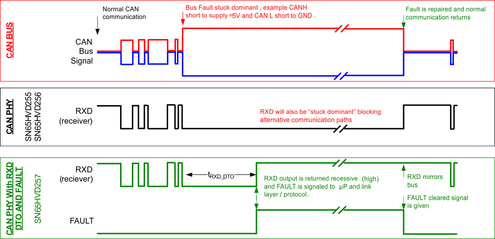 Figure 13. Example Timing Diagram for Devices With and Without RXD DTO and FAULT Terminal
9.3.1.5 Unpowered Device
The device is designed to be an 'ideal passive' or 'no load' to the CAN bus if it is unpowered. The bus terminals (CANH, CANL) have extremely low leakage currents when the device is unpowered so they will not load down the bus. This is critical if some nodes of the network will be unpowered while the rest of the of network remains in operation. The logic terminals also have extremely low leakage currents when the device is unpowered to avoid loading down other circuits that may remain powered.
9.3.1.6 Floating Terminals
The device has internal pull ups and pull downs on critical terminals to place the device into known states if the terminals float. The TXD terminal is pulled up to VCC to force a recessive input level if the terminal floats. The S terminal is pulled down to GND to force the device into normal mode if the terminal floats.
9.3.1.7 CAN Bus Short Circuit Current Limiting
The device has several protection features that limit the short circuit current when a CAN bus line is shorted. These include driver current limiting (dominant and recessive). The device has TXD dominant state time out to prevent permanent higher short circuit current of the dominant state during a system fault. During CAN communication the bus switches between dominant and recessive states with the data and control fields bits, thus the short circuit current may be viewed either as the instantaneous current during each bus state, or as a DC average current. For system current (power supply) and power considerations in the termination resistors and common-mode choke ratings, use the average short circuit current. Determine the ratio of dominant and recessive bits by the data in the CAN frame plus the following factors of the protocol and PHY that force either recessive or dominant at certain times:
- Control fields with set bits
- Bit stuffing
- Interframe space
- TXD dominant time out (fault case limiting)
NOTE
The short circuit current of the bus depends on the ratio of recessive to dominant bits and their respective short circuit currents. The average short circuit current may be calculated with the following formula:
Where:
- IOS(AVG) is the average short circuit current
- %Transmit is the percentage the node is transmitting CAN messages
- %Receive is the percentage the node is receiving CAN messages
- %REC_Bits is the percentage of recessive bits in the transmitted CAN messages
- %DOM_Bits is the percentage of dominant bits in the transmitted CAN messages
- IOS(SS)_REC is the recessive steady state short circuit current
- IOS(SS)_DOM is the dominant steady state short circuit current
NOTE
Consider the short circuit current and possible fault cases of the network when sizing the power ratings of the termination resistance and other network components.
9.4 Device Functional Modes
The device has two main operating modes: normal mode and silent mode. Operating mode selection is made via the S input terminal.
Table 4. Operating Modes
| S Terminal | MODE | DRIVER | RECEIVER | RXD Terminal |
|---|---|---|---|---|
| LOW | Normal Mode | Enabled (ON) | Enabled (ON) | Mirrors Bus State(1) |
| HIGH | Silent Mode | Disabled (OFF) | Enabled (ON) | Mirrors Bus State |
9.4.1 Can Bus States
The CAN bus has two states during powered operation of the device; dominant and recessive. A dominant bus state is when the bus is driven differentially, corresponding to a logic low on the TXD and RXD terminal. A recessive bus state is when the bus is biased to VCC / 2 via the high-resistance internal input resistors RIN of the receiver, corresponding to a logic high on the TXD and RXD terminals. See Figure 14 and Figure 15.
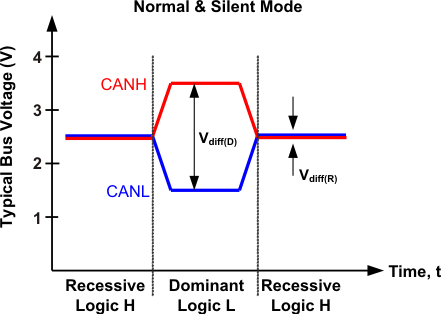 Figure 14. Bus States (Physical Bit Representation)
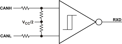 Figure 15. Bias Unit (Recessive Common Mode Bias) and Receiver
9.4.2 Normal Mode
Select the normal mode of device operation by setting S low. The CAN driver and receiver are fully operational and CAN communication is bi-directional. The driver is translating a digital input on TXD to a differential output on CANH and CANL. The receiver is translating the differential signal from CANH and CANL to a digital output on RXD.
9.4.3 Silent Mode
Activate silent mode (receive only) by setting S high. The CAN driver is turned off while the receiver remains active and RXD outputs the received bus state.
NOTE
Silent mode may be used to implement babbling idiot protection, to ensure that the driver does not disrupt the network during a local fault. Silent mode may also be used in redundant systems to select or de-select the redundant transceiver (driver) when needed.
9.4.4 Driver and Receiver Function Tables
Table 5. Driver Function Table
| DEVICE | INPUTS | OUTPUTS | DRIVEN BUS STATE | ||
|---|---|---|---|---|---|
| S(1) (2) | TXD(1) (3) | CANH(1) | CANL(1) | ||
| All Devices | L or Open | L | H | L | Dominant |
| H or Open | Z | Z | Recessive | ||
| H | X | Z | Z | Recessive | |
Table 6. Receiver Function Table
| DEVICE MODE | CAN DIFFERENTIAL INPUTS VID = VCANH – VCANL |
BUS STATE | RXD TERMINAL(1) |
|---|---|---|---|
| Normal or Silent | VID ≥ 0.9 V | Dominant | L(2) |
| 0.5 V < VID < 0.9 V | ? | ? | |
| VID ≤ 0.5 V | Recessive | H | |
| Open (VID ≈ 0 V) | Open | H |
9.4.5 Digital Inputs and Outputs
9.4.5.1 5-V VCC Only Devices (SN65HVD265 and SN65HVD267)
The 5-V VCC device is supplied by a single 5-V rail. The digital inputs are 5 V and 3.3 V compatible. This device has a 5-V (VCC) level RXD output. TXD is internally pulled up to VCC and S is internally pulled down to GND.
NOTE
TXD is internally pulled up to VCC and the S terminal is internally pulled down to GND. However, the internal bias may only put the device into a known state if the terminals float. The internal bias may be inadequate for system-level biasing. TXD pullup strength and CAN bit timing require special consideration when the SN65HVD26x devices are used with an open-drain TXD output on the CAN controller. An adequate external pullup resistor must be used to ensure that the CAN controller output of the μP maintains adequate bit timing input to the SN65HVD26x.
9.4.5.2 5-V VCC with VRXD RXD Output Supply Devices (SN65HVD266)
This device is a 5-V VCC CAN transceiver with a separate supply for the RXD output, VRXD. The digital inputs are 5 V and 3.3 V compatible. These devices have a VRXD-level RXD output. TXD remains weakly pulled up to VCC.
NOTE
On device versions with a VRXD supply that shifts the RXD output level, the input terminals of the device remain the same. TXD remains weakly pulled up to VCC internally. Thus, a small IIH current flows if the TXD input is used below VCC levels.
9.4.5.3 5-V VCC with FAULT Open-Drain Output Device (SN65HVD267)
This device has a FAULT output terminal (open-drain). FAULT must be pulled up to VCC or I/O supply level via an external resistor.
NOTE
Because the FAULT output terminal is open-drain, it actively pulls down when there is no fault, and becomes high-impedance when a fault condition is detected. An external pullup resistor to the VCC or I/O supply of the system must be used to pull the terminal high to indicate a fault to the host microprocessor. The open-drain architecture makes the fault terminal compatible with 3.3 V and 5 V I/O-level systems. The pullup current, selected by the pullup resistance value, should be as low as possible while achieving the desired voltage level output in the system with margin against noise.
