SGLS367E September 2006 – September 2015 SN65HVD30-EP , SN65HVD33-EP
PRODUCTION DATA.
- 1 Features
- 2 Applications
- 3 Description
- 4 Revision History
- 5 Pin Configuration and Functions
-
6 Specifications
- 6.1 Absolute Maximum Ratings
- 6.2 ESD Ratings
- 6.3 Recommended Operating Conditions
- 6.4 Thermal Information
- 6.5 Electrical Characteristics: Driver
- 6.6 Electrical Characteristics: Receiver
- 6.7 Switching Characteristics: Driver
- 6.8 Switching Characteristics: Receiver
- 6.9 Receiver Equalization Characteristics
- 6.10 Dissipation Ratings
- 6.11 Typical Characteristics
- 7 Parameter Measurement Information
- 8 Detailed Description
- 9 Application and Implementation
- 10Power Supply Recommendations
- 11Layout
- 12Device and Documentation Support
- 13Mechanical, Packaging, and Orderable Information
Package Options
Mechanical Data (Package|Pins)
- D|8
Thermal pad, mechanical data (Package|Pins)
- D|8
Orderable Information
6 Specifications
6.1 Absolute Maximum Ratings
over operating free-air temperature range (unless otherwise noted)(1) (2)| MIN | MAX | UNIT | ||||
|---|---|---|---|---|---|---|
| VCC | Supply voltage range | –0.3 | 6 | V | ||
| V(A), V(B), V(Y), V(Z) | Voltage range at any bus terminal (A, B, Y, Z) | –9 | 14 | V | ||
| V(TRANS) | Voltage input, transient pulse through 100 Ω (see Figure 21) (A, B, Y, Z)(3) | –50 | 50 | V | ||
| VI | Input voltage range (D, DE, RE) | –0.5 | 7 | V | ||
| PD(cont) | Continuous total power dissipation | Internally limited(4) | ||||
| IO | Output current (receiver output only, R) | 11 | mA | |||
| TJ | Junction temperature | 165 | °C | |||
| Tstg | Storage temperature range | –65 | 150 | °C | ||
(1) Stresses beyond those listed under absolute maximum ratings may cause permanent damage to the device. These are stress ratings only, and functional operation of the device at these or any other conditions beyond those indicated under recommended operating conditions is not implied. Exposure to absolute-maximum-rated conditions for extended periods may affect device reliability.
(2) All voltage values, except differential I/O bus voltages, are with respect to network ground terminal.
(3) This tests survivability only and the output state of the receiver is not specified.
(4) The thermal shutdown protection circuit internally limits the continuous total power dissipation. Thermal shutdown typically occurs when the junction temperature reaches 165°C.
6.2 ESD Ratings
| MIN | UNIT | ||||
|---|---|---|---|---|---|
| V(ESD) | Electrostatic discharge | Human body model (HBM), per ANSI/ESDA/JEDEC JS-001, all pins(1) | Bus pins and GND | ±16000 | V |
| All pins | ±4000 | ||||
| Charged device model (CDM), per JEDEC specification JESD22-C101, all pins(2) | ±1000 | ||||
(1) JEDEC document JEP155 states that 500-V HBM allows safe manufacturing with a standard ESD control process.
(2) JEDEC document JEP157 states that 250-V CDM allows safe manufacturing with a standard ESD control process.
6.3 Recommended Operating Conditions
over operating free-air temperature range (unless otherwise noted)| MIN | NOM | MAX | UNIT | ||||
|---|---|---|---|---|---|---|---|
| VCC | Supply voltage | 3 | 3.6 | V | |||
| VI or VIC | Voltage at any bus terminal (separately or common mode) | –7(1) | 12 | V | |||
| 1/tUI | Signaling rate | 'HVD30, 'HVD33 | 25 | Mbps | |||
| 'HVD31, 'HVD34 | 5 | ||||||
| 'HVD32, 'HVD35 | 1 | ||||||
| RL | Differential load resistance | 54 | 60 | Ω | |||
| VIH | High-level input voltage | D, DE, RE | 2 | VCC | V | ||
| VIL | Low-level input voltage | D, DE, RE | 0 | 0.8 | V | ||
| VID | Differential input voltage | –12 | 12 | V | |||
| IOH | High-level output current | Driver | –60 | mA | |||
| Receiver | –8 | ||||||
| IOL | Low-level output current | Driver | 60 | mA | |||
| Receiver | 8 | ||||||
| TA | Ambient still-air temperature | –55 | 125(2) | °C | |||
(1) The algebraic convention, in which the least positive (most negative) limit is designated as minimum, is used in this data sheet.
(2) Long-term high-temperature storage and/or extended use at maximum recommended operating conditions may result in a reduction of overall device life. See http://www.ti.com/ep_quality for additional information on enhanced plastic packaging.
6.4 Thermal Information
| THERMAL METRIC(1) | D (SOIC) | D (SOIC) | UNIT | |
|---|---|---|---|---|
| 8 PINS | 14 PINS | |||
| RθJA | Junction-to-ambient thermal resistance | 135 | 92 | °C/W |
| RθJC(top) | Junction-to-case (top) thermal resistance | 43 | 59 | °C/W |
| RθJB | Junction-to-board thermal resistance | 44 | 61 | °C/W |
| ψJT | Junction-to-top characterization parameter | 12.1 | 5.7 | °C/W |
| ψJB | Junction-to-board characterization parameter | 49.7 | 30.7 | °C/W |
| RθJC(bot) | Junction-to-case (bottom) thermal resistance | — | — | °C/W |
(1) For more information about traditional and new thermal metrics, see the IC Package Thermal Metrics application report, SPRA953.
6.5 Electrical Characteristics: Driver
over recommended operating conditions (unless otherwise noted)| PARAMETER | TEST CONDITIONS | MIN | TYP(1) | MAX | UNIT | |||
|---|---|---|---|---|---|---|---|---|
| VI(K) | Input clamp voltage | II = –18 mA | –1.5 | V | ||||
| |VOD(SS)| | Steady-state differential output voltage | IO = 0 | 2.3 | VCC + 0.1 | V | |||
| RL = 54 Ω, See Figure 10 (RS-485) | 1.5 | 2 | ||||||
| RL = 100 Ω, See Figure 10 (RS-422) | 2 | 2.3 | ||||||
| Vtest = –7 V to 12 V, See Figure 11 | 1.5 | |||||||
| Δ|VOD(SS)| | Change in magnitude of steady-state differential output voltage between states | RL = 54 Ω, See Figure 10 and Figure 11 | –0.2 | 0.2 | V | |||
| VOD(RING) | Differential output voltage overshoot and undershoot | RL = 54 Ω, CL = 50 pF, See Figure 14 and Figure 12 | 10%(2) | V | ||||
| VOC(PP) | Peak-to-peak common-mode output voltage | 'HVD30, 'HVD33 | See Figure 13 | 0.5 | V | |||
| 'HVD31, 'HVD32, 'HVD34, 'HVD35 | 0.25 | |||||||
| VOC(SS) | Steady-state common-mode output voltage | See Figure 13 | 1.6 | 2.3 | V | |||
| ΔVOC(SS) | Change in steady-state common-mode output voltage | See Figure 13 | –0.05 | 0.05 | V | |||
| IZ(Z) or IY(Z) |
High-impedance state output current | 'HVD30, 'HVD31, 'HVD32 | VCC = 0 V, VZ or VY = 12 V, Other input at 0 V |
90 | μA | |||
| VCC = 0 V, VZ or VY = –7 V, Other input at 0 V |
–10 | |||||||
| 'HVD33, 'HVD34, 'HVD35 | VCC = 3 V or 0 V, DE = 0 V, VZ or VY = 12 V |
Other input at 0 V |
90 | |||||
| VCC = 3 V or 0 V, DE = 0 V, VZ or VY = –7 V |
–10 | |||||||
| IZ(S) or IY(S) |
Short-circuit output current | VZ or VY = –7 V | Other input at 0 V |
±250 | mA | |||
| VZ or VY = 12 V | ||||||||
| II | Input current | D, DE | 0 | 100 | μA | |||
| C(OD) | Differential output capacitance | VOD = 0.4 sin (4E6πt) + 0.5 V, DE at 0 V | 16 | pF | ||||
(1) All typical values at 25°C with 3.3-V supply
(2) 10% of the peak-to-peak differential output voltage swing, per TIA/EIA-485
6.6 Electrical Characteristics: Receiver
over recommended operating conditions (unless otherwise noted)| PARAMETER | TEST CONDITIONS | MIN | TYP(1) | MAX | UNIT | |||||
|---|---|---|---|---|---|---|---|---|---|---|
| VIT+ | Positive-going differential input threshold voltage | IO = –8 mA | –0.02 | V | ||||||
| VIT– | Negative-going differential input threshold voltage | 'HVD30 | IO = 8 mA | –0.15 | V | |||||
| 'HVD33 | -0.2 | |||||||||
| Vhys | Hysteresis voltage (VIT+ – VIT–) | 50 | mV | |||||||
| VIK | Enable-input clamp voltage | II = –18 mA | –1.5 | V | ||||||
| VO | Output voltage | VID = 200 mV, IO = –8 mA, See Figure 17 | 2.4 | V | ||||||
| VID = –200 mV, IO = 8 mA, See Figure 17 | 0.4 | |||||||||
| IO(Z) | High-impedance-state output current | VO = 0 or VCC, RE at VCC | –1 | 1 | μA | |||||
| IA or IB | Bus input current | 'HVD31, 'HVD32, 'HVD34, 'HVD35 |
VA or VB = 12 V | Other input at 0 V |
0.05 | 0.1 | mA | |||
| VA or VB = 12 V, VCC = 0 V | 0.06 | 0.1 | ||||||||
| VA or VB = –7 V | –0.10 | –0.04 | ||||||||
| VA or VB = –7 V, VCC = 0 V | –0.10 | –0.03 | ||||||||
| 'HVD30, 'HVD33 | VA or VB = 12 V | Other input at 0 V |
0.20 | 0.35 | ||||||
| VA or VB = 12 V, VCC = 0 V | 0.24 | 0.4 | ||||||||
| VA or VB = –7 V | –0.35 | –0.18 | ||||||||
| VA or VB = –7 V, VCC = 0 V | –0.25 | –0.13 | ||||||||
| IIH | Input current, RE | VIH = 0.8 V or 2 V | –60 | μA | ||||||
| CID | Differential input capacitance | VID = 0.4 sin (4E6πt) + 0.5 V, DE at 0 V | 15 | pF | ||||||
| SUPPLY CURRENT | ||||||||||
| ICC | Supply current | 'HVD30 | D at 0 V or VCC and no load | 2.1 | mA | |||||
| 'HVD31, 'HVD32 | 6.4 | |||||||||
| 'HVD33 | RE at 0 V, D at 0 V or VCC, DE at 0 V, No load (receiver enabled and driver disabled) |
1.8 | ||||||||
| 'HVD34, 'HVD35 | 2.2 | |||||||||
| 'HVD33, 'HVD34, 'HVD35 | RE at VCC, D at VCC, DE at 0 V, No load (receiver disabled and driver disabled) |
0.022 | 1.5 | μA | ||||||
| 'HVD33 | RE at 0 V, D at 0 V or VCC, DE at VCC, No load (receiver enabled and driver enabled) |
2.1 | mA | |||||||
| 'HVD34, 'HVD35 | 6.5 | |||||||||
| 'HVD33 | RE at VCC, D at 0 V or VCC, DE at VCC
No load (receiver disabled and driver enabled) |
1.8 | ||||||||
| 'HVD34, 'HVD35 | 6.2 | |||||||||
(1) All typical values at 25°C with 3.3-V supply
6.7 Switching Characteristics: Driver
over recommended operating conditions (unless otherwise noted)| PARAMETER | TEST CONDITIONS | MIN | TYP(1) | MAX | UNIT | ||
|---|---|---|---|---|---|---|---|
| tPLH | Propagation delay time, low- to high-level output |
'HVD30, 'HVD33 | RL = 54 Ω, CL = 50 pF, See Figure 14 |
4 | 10 | 23 | ns |
| 'HVD31, 'HVD34 | 25 | 38 | 65 | ||||
| 'HVD32, 'HVD35 | 120 | 175 | 305 | ||||
| tPHL | Propagation delay time, high- to low-level output |
'HVD30, 'HVD33 | 4 | 9 | 23 | ns | |
| 'HVD31, 'HVD34 | 25 | 38 | 65 | ||||
| 'HVD32, 'HVD35 | 120 | 175 | 305 | ||||
| tr | Differential output signal rise time |
'HVD30, 'HVD33 | 2.5 | 5 | 18 | ns | |
| 'HVD31, 'HVD34 | 20 | 37 | 60 | ||||
| 'HVD32, 'HVD35 | 120 | 185 | 300 | ||||
| tf | Differential output signal fall time |
'HVD30, 'HVD33 | 2.5 | 5 | 18 | ns | |
| 'HVD31, 'HVD34 | 20 | 35 | 60 | ||||
| 'HVD32, 'HVD35 | 120 | 180 | 300 | ||||
| tsk(p) | Pulse skew (|tPHL – tPLH|) | 'HVD30, 'HVD33 | 0.6 | ns | |||
| 'HVD31, 'HVD34 | 2.0 | ||||||
| 'HVD32, 'HVD35 | 5.1 | ||||||
| tPZH1 | Propagation delay time, high-impedance to high-level output | 'HVD33 | RL = 110 Ω, RE at 0 V, D = 3 V and S1 = Y, or D = 0 V and S1 = Z, See Figure 15 |
45 | ns | ||
| 'HVD34 | 235 | ||||||
| 'HVD35 | 490 | ||||||
| tPHZ | Propagation delay time, high-level to high-impedance output | 'HVD33 | 25 | ns | |||
| 'HVD34 | 65 | ||||||
| 'HVD35 | 165 | ||||||
| tPZL1 | Propagation delay time, high-impedance to low-level output | 'HVD33 | RL = 110 Ω, RE at 0 V, D = 3 V and S1 = Z, or D = 0 V and S1 = Y, See Figure 16 |
35 | ns | ||
| 'HVD34 | 190 | ||||||
| 'HVD35 | 490 | ||||||
| tPLZ | Propagation delay time, low-level to high-impedance output | 'HVD33 | 30 | ns | |||
| 'HVD34 | 120 | ||||||
| 'HVD35 | 290 | ||||||
| tPZH2 | Propagation delay time, standby to high-level output | 'HVD30 | RL = 110 Ω, RE at 3 V, D = 3 V and S1 = Y, or D = 0 V and S1 = Z, See Figure 15 |
4000 | ns | ||
| 'HVD33 | 5000 | ||||||
| tPZL2 | Propagation delay time, standby to low-level output | 'HVD30 | RL = 110 Ω, RE at 3 V, D = 3 V and S1 = Z, or D = 0 V and S1 = Y, See Figure 16 |
4000 | ns | ||
| 'HVD33 | 5000 | ||||||
(1) All typical values at 25°C with 3.3-V supply
6.8 Switching Characteristics: Receiver
over operating free-air temperature range (unless otherwise noted)| PARAMETER | TEST CONDITIONS | MIN | TYP | MAX | UNIT | |||
|---|---|---|---|---|---|---|---|---|
| tPLH | Propagation delay time, low- to high-level output |
'HVD30, 'HVD33 | VID = –1.5 V to 1.5 V, CL = 15 pF, See Figure 18 |
26 | 60 | ns | ||
| 'HVD31, 'HVD32, 'HVD34, 'HVD35 | 47 | 70 | ||||||
| tPLH | Propagation delay time, high- to low-level output |
'HVD30, 'HVD33 | 29 | 60 | ns | |||
| 'HVD31, 'HVD32, 'HVD34, 'HVD35 | 49 | 70 | ||||||
| tsk(p) | Pulse skew (|tPHL – tPLH|) | 'HVD30, 'HVD33 | 12 | ns | ||||
| 'HVD31, 'HVD34, 'HVD32, 'HVD35 | 10 | |||||||
| tr | Output signal rise time | 'HVD30 | 10 | ns | ||||
| 'HVD33 | 18 | |||||||
| tf | Output signal fall time | 12.5 | ns | |||||
| tPHZ | Output disable time from high level | DE at 3 V | CL = 15 pF, See Figure 19 |
20 | ns | |||
| tPZH1 | Output enable time to high level | 20 | ns | |||||
| tPZH2 | Propagation delay time, standby to high-level output | 'HVD30 | DE at 0 V | 4000 | ns | |||
| 'HVD33 | 5000 | |||||||
| tPLZ | Output disable time from low level | DE at 3 V | CL = 15 pF, See Figure 20 |
20 | ns | |||
| tPZL1 | Output enable time to low level | 20 | ns | |||||
| tPZL2 | Propagation delay time, standby to low-level output | 'HVD30 | DE at 0 V | 4000 | ns | |||
| 'HVD33 | 5000 | ns | ||||||
6.9 Receiver Equalization Characteristics
over recommended operating conditions (unless otherwise noted)| PARAMETER | TEST CONDITIONS | DEVICE | MIN | TYP(1) | MAX | UNIT | |||
|---|---|---|---|---|---|---|---|---|---|
| tj(pp) | Peak-to-peak eye-pattern jitter |
Pseudo-random NRZ code with a bit pattern length of 216 – 1, Belden 3105A cable | 25 Mbps | 100 m | 'HVD33(2) | PREVIEW | ns | ||
| 150 m | 'HVD33(2) | PREVIEW | |||||||
| 200 m | 'HVD33(2) | PREVIEW | |||||||
| 10 Mbps | 200 m | 'HVD33(2) | PREVIEW | ||||||
| 250 m | 'HVD33(2) | PREVIEW | |||||||
| 300 m | 'HVD33(2) | PREVIEW | |||||||
| 5 Mbps | 500 m | 'HVD34(2) | PREVIEW | ||||||
| 3 Mbps | 500 m | 'HVD33(2) | PREVIEW | ||||||
| 'HVD34(2) | PREVIEW | ||||||||
| 1 Mbps | 1000 m | 'HVD34(2) | PREVIEW | ||||||
(1) All typical values are at VCC = 5 V and temperature = 25°C.
(2) The SN65HVD33-EP and the SN65HVD34-EP do not have receiver equalization, but are specified for comparison.
6.10 Dissipation Ratings
| PARAMETER | DEVICE | TEST CONDITIONS | MIN | MAX | UNIT |
|---|---|---|---|---|---|
| PD | 'HVD30 (25 Mbps) | RL = 60 Ω, CL = 50 pF, Input to D a 50% duty cycle square wave at indicated signaling rate, TA = 85°C |
197 | mW | |
| 'HVD31 (5 Mbps) | 213 | ||||
| 'HVD32 (1 Mbps) | 193 | ||||
| 'HVD33 (25 Mbps) | RL = 60 Ω, CL = 50 pF, DE at VCC, RE at 0 V, Input to D a 50% duty cycle square wave at indicated signaling rate, TA = 85°C |
197 | mW | ||
| 'HVD34 (5 Mbps) | 193 | ||||
| 'HVD35 (1 Mbps) | 248 |
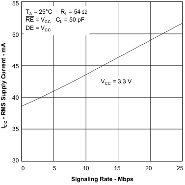
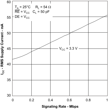
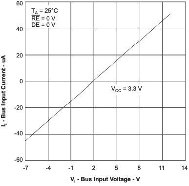
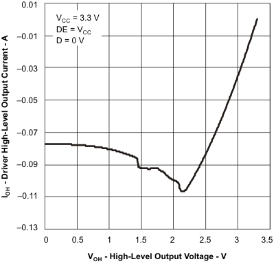
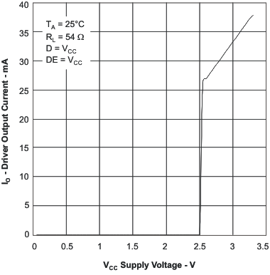
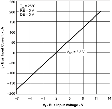
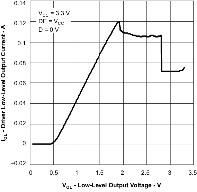
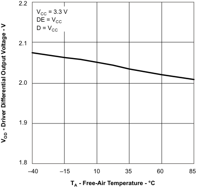
6.11 Typical Characteristics
