SLLS771F November 2006 – March 2023 SN65HVD3080E , SN65HVD3083E , SN65HVD3086E
PRODUCTION DATA
- 1 Features
- 2 Applications
- 3 Description
- 4 Revision History
-
5 Specifications
- 5.1 Absolute Maximum Ratings
- 5.2 Power Dissipation Ratings
- 5.3 Electrostatic Discharge Protection
- 5.4 Supply Current
- 5.5 Recommended Operating Conditions
- 5.6 Thermal Information
- 5.7 Driver Electrical Characteristics
- 5.8 Driver Switching Characteristics
- 5.9 Receiver Electrical Characteristics
- 5.10 Receiver Switching Characteristics
- 5.11 Typical Characteristics
- 6 Parameter Measurement Information
- 7 Device Information
- 8 Application Information
- 9 Device and Documentation Support
- 10Mechanical, Packaging, and Orderable Information
Package Options
Mechanical Data (Package|Pins)
Thermal pad, mechanical data (Package|Pins)
- D|14
Orderable Information
3 Description
Each of these devices is a balanced driver and receiver designed for full-duplex RS-485 or RS-422 data bus networks. Powered by a 5-V supply, they are fully compliant with the TIA/EIA-485A standard.
With controlled bus output transition times, the devices are suitable for signaling rates from 200 kbps to 20 Mbps.
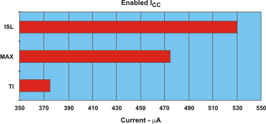
The devices are designed to operate with a low supply current, less than 1 mA (typical), exclusive of the load. When in the inactive shutdown mode, the supply current drops to a few nanoamps, making these devices ideal for power-sensitive applications.
The wide common-mode range and high ESD protection levels of these devices make them suitable for demanding applications such as motion controllers, electrical inverters, industrial networks, and cabled chassis interconnects where noise tolerance is essential.
These devices are characterized for operation over the temperature range -40°C to 85°C
| PART NUMBER | SIGNALING RATE | PACKAGE(1) |
|---|---|---|
| SN65HVD3080E | 200 kbps | DGS, DGSR 10-pin MSOP(2) |
| SN65HVD3083E | 1 Mbps | |
| SN65HVD3086E | 20 Mbps | |
| D 14-pin SOIC |