SLLS665M September 2005 – February 2023 SN65HVD30 , SN65HVD31 , SN65HVD32 , SN65HVD33 , SN65HVD34 , SN65HVD35
PRODUCTION DATA
- 1 Features
- 2 Applications
- 3 Description
- 4 Revision History
- 5 Device Comparison
- 6 Pin Configuration and Functions
-
7 Specifications
- 7.1 Absolute Maximum Ratings
- 7.2 ESD Ratings
- 7.3 Recommended Operating Conditions
- 7.4 Thermal Information
- 7.5 Electrical Characteristics: Driver
- 7.6 Electrical Characteristics: Receiver
- 7.7 Device Power Dissipation – PD
- 7.8 Supply Current Characteristics
- 7.9 Switching Characteristics: Driver
- 7.10 Switching Characteristics: Receiver
- 7.11 Dissipation Ratings
- 7.12 Typical Characteristics
- 8 Detailed Description
- 9 Application and Implementation
- 10Device and Documentation Support
- 11Mechanical, Packaging, and Orderable Information
Package Options
Mechanical Data (Package|Pins)
- D|14
Thermal pad, mechanical data (Package|Pins)
- D|14
Orderable Information
8.4 Device Functional Modes
Table 8-1 SN65HVD33, SN65HVD34, SN65HVD35 Driver
| INPUTS | OUTPUTS | ||
|---|---|---|---|
| D | DE | Y | Z |
| H | H | H | L |
| L | H | L | H |
| X | L or open | Z | Z |
| Open | H | L | H |
Table 8-2 SN65HVD33, SN65HVD34, SN65HVD35 Receiver
| DIFFERENTIAL INPUTS VID = V(A) – V(B) | ENABLE RE | OUTPUT R |
|---|---|---|
| VID ≤ –0.2 V | L | L |
| –0.2 V < VID < –0.02 V | L | ? |
| –0.02 V ≤ VID | L | H |
| X | H or open | Z |
| Open Circuit | L | H |
| Idle circuit | L | H |
| Short Circuit, V(A) = V(B) | L | H |
Table 8-3 SN65HVD30, SN65HVD31, SN65HVD32 Driver
| INPUT D | OUTPUTS | |
|---|---|---|
| Y | Z | |
| H | H | L |
| L | L | H |
| Open | L | H |
Table 8-4 SN65HVD30, SN65HVD31, SN65HVD32 Receiver
| DIFFERENTIAL INPUTS VID = V(A) – V(B) | OUTPUT R |
|---|---|
| VID ≤ –0.2 V | L |
| –0.2 V < VID < –0.02 V | ? |
| –0.02 V ≤ VID | H |
| Open Circuit | H |
| Idle circuit | H |
| Short Circuit, V(A) = V(B) | H |
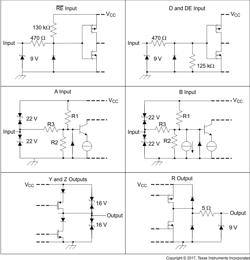
 Figure 8-5 Equivalent Input and Output Schematic Diagrams
Table 8-5 Input Attenuator Resistance Values
| PART NUMBER | R1, R2 | R3 |
|---|---|---|
| SN65HVD30, SN65HVD33 | 9 kΩ | 45 kΩ |
| SN65HVD31, SN65HVD32, SN65HVD34, SN65HVD35 | 36 kΩ | 180 kΩ |