SLLS665M September 2005 – February 2023 SN65HVD30 , SN65HVD31 , SN65HVD32 , SN65HVD33 , SN65HVD34 , SN65HVD35
PRODUCTION DATA
- 1 Features
- 2 Applications
- 3 Description
- 4 Revision History
- 5 Device Comparison
- 6 Pin Configuration and Functions
-
7 Specifications
- 7.1 Absolute Maximum Ratings
- 7.2 ESD Ratings
- 7.3 Recommended Operating Conditions
- 7.4 Thermal Information
- 7.5 Electrical Characteristics: Driver
- 7.6 Electrical Characteristics: Receiver
- 7.7 Device Power Dissipation – PD
- 7.8 Supply Current Characteristics
- 7.9 Switching Characteristics: Driver
- 7.10 Switching Characteristics: Receiver
- 7.11 Dissipation Ratings
- 7.12 Typical Characteristics
- 8 Detailed Description
- 9 Application and Implementation
- 10Device and Documentation Support
- 11Mechanical, Packaging, and Orderable Information
Package Options
Mechanical Data (Package|Pins)
- D|14
Thermal pad, mechanical data (Package|Pins)
- D|14
Orderable Information
3 Description
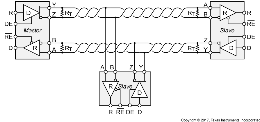
The SN65HVD3x devices are 3-state differential line drivers and differential-input line receivers that operate with 3.3-V power supply.
Each driver and receiver has separate input and output pins for full-duplex bus communication designs. They are designed for RS-422 and RS-485 data transmission over cable lengths of up to
1500 meters.
The SN65HVD30, SN65HVD31, and SN65HVD32 devices are fully enabled with no external enabling pins.
The SN65HVD33, SN65HVD34, and SN65HVD35 devices have active-high driver enables and active-low receiver enables. A low, less than 1 μA, standby current can be achieved by disabling both the driver and receiver.
All devices are characterized for ambient temperatures from –40°C to 85°C. Low power dissipation allows operation at temperatures up to 105°C or 125°C, depending on package option.
| PART NUMBER | PACKAGE(1) | BODY SIZE (NOM) |
|---|---|---|
| SN65HVD30 | SOIC (8) | 4.90 mm × 3.91 mm |
| SN65HVD31 | ||
| SN65HVD32 | ||
| SN65HVD33 | SOIC (14) | 8.65 mm × 3.91 mm |
| VQFN (20) | 4.50 mm × 3.50 mm | |
| SN65HVD34 | SOIC (14) | 8.65 mm × 3.91 mm |
| SN65HVD35 |
 Typical Application Schematic