SLLS665M September 2005 – February 2023 SN65HVD30 , SN65HVD31 , SN65HVD32 , SN65HVD33 , SN65HVD34 , SN65HVD35
PRODUCTION DATA
- 1 Features
- 2 Applications
- 3 Description
- 4 Revision History
- 5 Device Comparison
- 6 Pin Configuration and Functions
-
7 Specifications
- 7.1 Absolute Maximum Ratings
- 7.2 ESD Ratings
- 7.3 Recommended Operating Conditions
- 7.4 Thermal Information
- 7.5 Electrical Characteristics: Driver
- 7.6 Electrical Characteristics: Receiver
- 7.7 Device Power Dissipation – PD
- 7.8 Supply Current Characteristics
- 7.9 Switching Characteristics: Driver
- 7.10 Switching Characteristics: Receiver
- 7.11 Dissipation Ratings
- 7.12 Typical Characteristics
- 8 Detailed Description
- 9 Application and Implementation
- 10Device and Documentation Support
- 11Mechanical, Packaging, and Orderable Information
Package Options
Mechanical Data (Package|Pins)
- D|14
Thermal pad, mechanical data (Package|Pins)
- D|14
Orderable Information
9.2 Typical Application
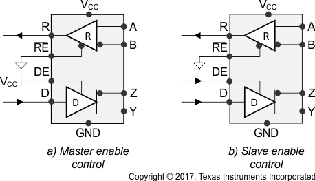
A full-duplex RS-485 network consists of multiple transceivers connecting in parallel to two bus cables. On one signal pair, a master driver transmits data to multiple slave receivers. The master driver and slave receivers can remain fully enabled at all times. On the other signal pair, multiple slave drivers transmit data to the master receiver. To avoid bus contention, the slave drivers must be intermittently enabled and disabled such that only one driver is enabled at any time, as in half-duplex communication. The master receiver can remain fully enabled at all times.
Because the driver cannot be disabled, only connect one driver to the bus when using the SN65HVD30, SN65HVD31, or SN65HVD32 devices.
 Figure 9-2 Full-Duplex Transceiver Configurations