SLLSE11H March 2012 – March 2019 SN65HVD72 , SN65HVD75 , SN65HVD78
UNLESS OTHERWISE NOTED, this document contains PRODUCTION DATA.
- 1 Features
- 2 Applications
- 3 Description
- 4 Revision History
- 5 Device Comparison Table
- 6 Pin Configuration and Functions
-
7 Specifications
- 7.1 Absolute Maximum Ratings
- 7.2 ESD Ratings
- 7.3 Recommended Operating Conditions
- 7.4 Thermal Information
- 7.5 Electrical Characteristics
- 7.6 Power Dissipation
- 7.7 Switching Characteristics: 250 kbps Device (SN65HVD72) Bit Time ≥ 4 µs
- 7.8 Switching Characteristics: 20 Mbps Device (SN65HVD75) Bit Time ≥50 ns
- 7.9 Switching Characteristics: 50 Mbps Device (SN65HVD78) Bit Time ≥20 ns
- 7.10 Typical Characteristics
- 8 Parameter Measurement Information
- 9 Detailed Description
- 10Application and Implementation
- 11Power Supply Recommendations
- 12Layout
- 13Device and Documentation Support
- 14Mechanical, Packaging, and Orderable Information
Package Options
Mechanical Data (Package|Pins)
Thermal pad, mechanical data (Package|Pins)
- DRB|8
Orderable Information
9.4 Device Functional Modes
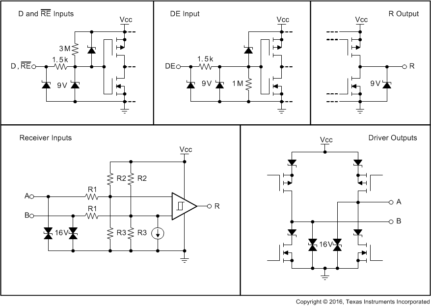
When the driver enable pin, DE, is logic high, the differential outputs A and B follow the logic states at data input D. A logic high at D causes A to turn high and B to turn low. In this case the differential output voltage defined as VOD = VA – VB is positive. When D is low, the output states reverse, B turns high, A becomes low, and VOD is negative.
When DE is low, both outputs turn high-impedance. In this condition the logic state at D is irrelevant. The DE pin has an internal pulldown resistor to ground; thus, when left open, the driver is disabled (high-impedance) by default. The D pin has an internal pullup resistor to VCC; thus, when left open while the driver is enabled, output A turns high and B turns low.
Table 1. Driver Function Table
| INPUT | ENABLE | OUTPUTS | DESCRIPTION | |
|---|---|---|---|---|
| D | DE | A | B | |
| H | H | H | L | Actively drive bus high |
| L | H | L | H | Actively drive bus low |
| X | L | Z | Z | Driver disabled |
| X | OPEN | Z | Z | Driver disabled by default |
| OPEN | H | H | L | Actively drive bus high by default |
When the receiver enable pin, RE, is logic low, the receiver is enabled. When the differential input voltage defined as VID = VA – VB is positive and higher than the positive input threshold, VIT+, the receiver output, R, turns high. When VID is negative and lower than the negative input threshold, VIT–, the receiver output turns low. If VID is between VIT+ and VIT–, the output is indeterminate.
When RE is logic high or left open, the receiver output is high-impedance and the magnitude and polarity of VID are irrelevant. Internal biasing of the receiver inputs causes the output to go failsafe-high when the transceiver is disconnected from the bus (open-circuit), the bus lines are shorted (short-circuit), or the bus is not actively driven (idle bus).
Table 2. Receiver Function Table
| DIFFERENTIAL INPUT | ENABLE | OUTPUT | DESCRIPTION |
|---|---|---|---|
| VID = VA – VB | RE | R | |
| VIT+ < VID | L | H | Receive valid bus high |
| VIT– < VID < VIT+ | L | ? | Indeterminate bus state |
| VID < VIT– | L | L | Receive valid bus low |
| X | H | Z | Receiver disabled |
| X | OPEN | Z | Receiver disabled by default |
| Open-circuit bus | L | H | Failsafe high output |
| Short-circuit bus | L | H | Failsafe high output |
| Idle (terminated) bus | L | H | Failsafe high output |
 Figure 18. Equivalent Input and Output Circuit Diagrams