SLLSED6B October 2012 – November 2017 SN65HVD82
PRODUCTION DATA.
- 1 Features
- 2 Applications
- 3 Description
- 4 Revision History
- 5 Pin Configuration and Functions
- 6 Specifications
- 7 Parameter Measurement Information
- 8 Detailed Description
- 9 Application and Implementation
- 10Power Supply Recommendations
- 11Layout
- 12Device and Documentation Support
- 13Mechanical, Packaging, and Orderable Information
Package Options
Mechanical Data (Package|Pins)
- D|8
Thermal pad, mechanical data (Package|Pins)
Orderable Information
1 Features
- Bus I/O Protection
- Industrial Temperature Range –40°C to 85°C
- Large Receiver Hysteresis (60 mV Typical) for Noise Rejection
- Low-Power Consumption
- <1-µA Standby Current
- <1-mA Quiescent Current
- Signaling Rate Optimized for 250 kbps
- Create a Custom Design Using the SN65HVD82 With the WEBENCH® Power Designer
2 Applications
- Electrical Meters
- Building Automation
- Industrial Networks
- Security Electronics
3 Description
This device has robust drivers and receivers for demanding industrial applications. The bus pins are robust to ESD events, with high levels of protection to Human-Body Model, Air-Gap Discharge, and Contact Discharge specifications.
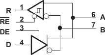
The device combines a differential driver and a differential receiver, which operate from a single 5-V power supply. The driver differential outputs and the receiver differential inputs are connected internally to form a bus port suitable for half-duplex (two-wire bus) communication. The device features a wide common-mode voltage range making the device suitable for multi-point applications over long cable runs. The device is characterized from –40°C to 85°C.
Device Information(1)
| PART NUMBER | PACKAGE | BODY SIZE (NOM) |
|---|---|---|
| SN65HVD82 | SOIC (8) | 4.90 mm × 3.91 mm |
- For all available packages, see the orderable addendum at the end of the datasheet.
Logic Diagram (Positive Logic)
