SLLS067I August 1990 – October 2022 SN55LBC176 , SN65LBC176 , SN75LBC176
PRODUCTION DATA
- 1 Features
- 2 Description
- 3 Revision History
- 4 Description (Continued)
- 5 Pin Configuration and Functions
-
6 Specifications
- 6.1 Absolute Maximum Ratings
- 6.2 Recommended Operating Conditions
- 6.3 Thermal Information: SN55LBC176
- 6.4 Thermal Information: SN65LBC176, SN75LBC176
- 6.5 Dissipation Ratings
- 6.6 Driver Electrical Characteristics
- 6.7 Driver Switching Characteristics
- 6.8 Receiver Electrical Characteristics
- 6.9 Receiver Switching Characteristics
- 7 Parameter Measurement Information
- 8 Detailed Description
- 9 Device and Documentation Support
- 10Mechanical, Packaging, and Orderable Information
Package Options
Mechanical Data (Package|Pins)
Thermal pad, mechanical data (Package|Pins)
Orderable Information
9.1.1 Thermal Characteristics of IC Packages
θJA (Junction-to-Ambient Thermal Resistance) is defined as the difference in junction temperature to ambient temperature divided by the operating power.
θJA is NOT a constant and is a strong function of
- the PCB design (50% variation)
- altitude (20% variation)
- device power (5% variation)
θJA can be used to compare the thermal performance of packages if the specific test conditions are defined and used. Standardized testing includes specification of PCB construction, test chamber volume, sensor locations, and the thermal characteristics of holding fixtures. θJA is often misused when it is used to calculate junction temperatures for other installations.
TI uses two test PCBs as defined by JEDEC specifications. The low-k board gives average in-use condition thermal performance and consists of a single trace layer 25 mm long and 2-oz thick copper. The high-k board gives best case in-use condition and consists of two 1-oz buried power planes with a single trace layer 25 mm long with 2-oz thick copper. A 4% to 50% difference in θJA can be measured between these two test cards.
θJC (Junction-to-Case Thermal Resistance) is defined as difference in junction temperature to case divided by the operating power. It is measured by putting the mounted package up against a copper block cold plate to force heat to flow from die, through the mold compound into the copper block.
θJC is a useful thermal characteristic when a heatsink is applied to package. It is NOT a useful characteristic to predict junction temperature as it provides pessimistic numbers if the case temperature is measured in a non-standard system and junction temperatures are backed out. It can be used with θJB in 1-dimensional thermal simulation of a package system.
θJB (Junction-to-Board Thermal Resistance) is defined to be the difference in the junction temperature and the PCB temperature at the center of the package (closest to the die) when the PCB is clamped in a cold−plate structure. θJB is only defined for the high-k test card.
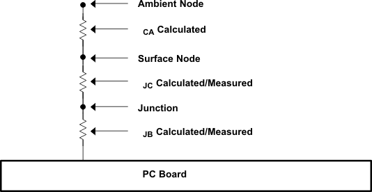
θJB provides an overall thermal resistance between the die and the PCB. It includes a bit of the PCB thermal resistance (especially for BGA’s with thermal balls) and can be used for simple 1-dimensional network analysis of package system (see Figure 9-1).
 Figure 9-1 Thermal Resistance