SLLS516E August 2002 – July 2015 SN65LVDS100 , SN65LVDS101 , SN65LVDT100 , SN65LVDT101
UNLESS OTHERWISE NOTED, this document contains PRODUCTION DATA.
- 1 Features
- 2 Applications
- 3 Description
- 4 Revision History
- 5 Description (Continued)
- 6 Device Options
- 7 Pin Configuration and Functions
- 8 Specifications
- 9 Parameter Measurement Information
- 10Detailed Description
-
11Application and Implementation
- 11.1 Application Information
- 11.2
Typical Application
- 11.2.1 PECL to LVDS Translation
- 11.2.2 LVDS to 3.3-V PECL Translation
- 11.2.3 5-V PECL to 3.3-V PECL Translation
- 11.2.4 CML to LVDS or 3.3-V PECL Translation
- 11.2.5 Single-Ended 3.3-V PECL to LVDS Translation
- 11.2.6 Single-Ended CMOS to LVDS Translation
- 11.2.7 Single-Ended CMOS to 3.3-V PECL Translation
- 11.2.8 Receipt of AC-Coupled Signals
- 12Power Supply Recommendations
- 13Layout
- 14Device and Documentation Support
- 15Mechanical, Packaging, and Orderable Information
Package Options
Refer to the PDF data sheet for device specific package drawings
Mechanical Data (Package|Pins)
- D|8
- DGK|8
Thermal pad, mechanical data (Package|Pins)
Orderable Information
10 Detailed Description
10.1 Overview
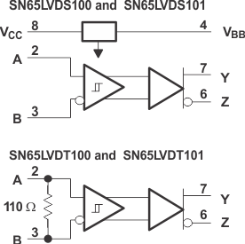
The SN65LVDx10x family of devices are fully differential, high-speed translators/repeaters. All devices in the family include a wide common-mode range receiver that accepts low-voltage differential signals covering a variety of standards. A receiver with an input sensitivity of ±100 mV and 25 mV of hysteresis is incorporated. The SN65LVDx100 devices include an output driver that meets all the specifications of the LVDS standard (TIA/EIA-644A). The SN65LVDx101 devices include an output driver that is compatible with 3.3-V PECL levels.
The SN65LVDx10x family is intended to drive a 100-Ω transmission line. This transmission line may be a printed-circuit board (PCB) or cabled interconnect. With transmission lines, optimum signal quality and power delivery is reached when a transmission line is terminated with a load equal to the characteristic impedance of the interconnecting media. Likewise, the driven 100-Ω transmission line should be terminated with a matched resistance.
10.2 Functional Block Diagram
10.3 Feature Description
10.3.1 Receiver Features
10.3.1.1 Voltage Range and Common-Mode Range
The receiver circuit incorporated into the SN65LVDx10x family supports receiving most low-voltage differential signals. This wide common-mode range receiver can accept any input signal between 0 and 4 V. Without referencing any specific standard, we can analyze the range of signals that can be input to this family of devices. Assuming an input signal has a 400-mV differential input voltage |(V+ – V–)|, the maximum recommended input voltage is 4 V. The absolute value of the most positive signal of a differential input would be VMAX:
where
- VCM = common-mode voltage
- VDIFF = differential voltage
Therefore, using our VMAX of 4 V and VDIFF of 400 mV, we see that we can simultaneously support a differential voltage of 400 mV and a common-mode voltage of 3.8 V. As is obvious from Equation 1, the common-mode and differential voltages are coupled: as the differential voltage increases in magnitude, the maximum common-mode voltage supported decreases.
Using a similar analysis, and considering the 0-V minimum input voltage, we can see that we could simultaneously support a differential voltage of 400 mV and a common-mode voltage of 0.2 V. Thus, we have a receiver that can support common-mode voltages in the approximate range of 0.2 V to 3.8 V.
The 400-mV example alluded to above is a reasonable maximum differential input voltage across a wide variety of standards (LVDS, M-LVDS, CML, LVPECL, and so on). We can use the specifications for any of these standards to understand the value of this wide input range receiver.
A standard compliant LVDS driver generates a 350-mV differential signal with a common-mode voltage of 1.2 V. The noninverting output thus resides at 1.375 V, while the inverting signal is at a voltage of 1.025 V. Because the SN65LVDx10x family receiver operates over a range of 0 V to 4 V, the wide common-mode receiver then can accept signals that are common-mode shifted by –1.025 V to 2.625 V. Similar analysis can be performed for any other input signal.
10.3.1.2 Sensitivity
Table 2 provides a truth table for the SN65LVDx10x family. Again, the same receiver circuitry is used on each of the devices in this family; therefore, the truth table is the same for all family devices. When the differential input voltage is greater than 100 mV, the receiver outputs a HI level. If the differential input voltage is less than –100 mV, the receiver outputs a LO level.
Between these two thresholds the receiver output is indeterminate. When the input signal falls in this –100 mV < VID < 100 mV range, the receiver output state cannot be determined unambiguously. Having said that, it is important to note that the SN65LVDx10x family receivers include 25 mV of hysteresis. The hysteresis is incorporated into the design to prevent the output switching when the receiver input voltage is close to 0 V (for example, the receiver inputs are open-circuited, or the receiver is connected to a driver that is high-impedance). With the open-circuited input and when the magnitude of the differential noise voltage on the bus is low (approximately < ±10 mV), the hysteresis serves to hold the device output at the last known state. This feature helps prevent chattering on the device output.
Noticeably absent from this receiver is any integrated failsafe feature. External components may be added to the receiver circuit to provide failsafe. Such an implementation is covered below.
10.3.1.3 Failsafe Considerations
Failsafe, in regard to a line receiver, usually means that the output goes to a defined logical state with no input signal. To keep added jitter to an absolute minimum, the SN65LVDS100 does not include this feature. It does exhibit 25 mV of input voltage hysteresis to prevent oscillation and keep the output in the last state prior to input-signal loss (assuming the differential noise in the system is less than the hysteresis).
Should failsafe be required, it may be added externally with a 1.6-kΩ pullup resistor to the 3.3-V supply and a 1.6-kΩ pulldown resistor to ground as shown in Figure 36 The default output state is determined by which line is pulled up or down and is the user's choice. The location of the 1.6-kΩ resistors is not critical. However, the 100-Ω resistor should be located at the end of the transmission line.
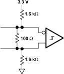 Figure 36. External Failsafe Circuit
Addition of this external failsafe will reduce the differential noise margin and add jitter to the output signal. The roughly 100-mV steady-state voltage generated across the 100-Ω resistor adds (or subtracts) from the signal generated by the upstream line driver. If the differential output of the line driver is symmetrical about zero volts, then the input at the receiver will appear asymmetrical with the external failsafe. Perhaps more important, is the extra time it takes for the input signal to overcome the added failsafe offset voltage.
In Figure 37 and using an external failsafe, the high-level differential voltage at the input of the SN65LVDS100 reaches 340 mV and the low-level –400 mV indicating a 60-mV differential offset induced by the external failsafe circuitry. The figure also reveals that the lowest peak-to-peak time jitter does not occur at zero-volt differential (the nominal input threshold of the receiver) but at –60 mV, the failsafe offset.
The added jitter from external failsafe increases as the signal transition times are slowed by cable effects. When a ten-meter CAT-5 UTP cable is introduced between the driver and receiver, the zero-crossing peak-to-peak jitter at the receiver output adds 250 ps when the external failsafe is added with this specific test set up. If external failsafe is used in conjunction with the SN65LVDS100, the noise margin and jitter effects should be budgeted.
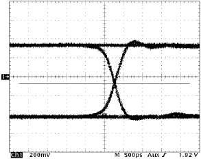 Figure 37. Receiver Input Eye Pattern with External Failsafe
10.3.1.4 VBB Voltage Reference
Pin 4 (VBB) on the SN65LVDS10x devices acts a voltage reference. This is an output signal from the device, with a nominal value of VCC – 1.35 V. This output can be used when receiving a single-ended input signal. This voltage reference would then be connected to the inverting input pin on the device (pin 3: B). The application where such a use makes sense is when the device is to receive a single-ended 3.3-V LVPECL signal. The common-mode voltage of a 3.3-V LVPECL signal is approximately 1.35 V below the device supply rail. While the value of VBB is ideal for single-ended LVPECL signals, its use may be extended to other single-ended inputs as long as the active single-ended signal is conditioned to have a common-mode voltage close to the nominal value of VBB.
Caution is in order when using the VBB signal. The expected application when using this signal is as a voltage reference to high-impedance input. The maximum current that can be sourced by this pin is 400 μA, while the maximum current that can be sunk is 12 μA. In cases where the SN65LVDS10x device is to be used without using VBB as a reference, the VBB pin should be left unconnected.
10.3.1.5 Integrated Termination
The SN65LVDT10x devices are identical to the SN65LVDS10x devices in all regards, with the addition that the SN65LVDT10x devices incorporate an integrated termination resistor along with the receiver. This termination would take the place of the matched load-line termination mentioned above. The SN65LVDT10x can be used in a point-to-point system or in a multidrop system when it is the last receiver on the multidrop bus. The SN65LVDT10x should not be used at every node in a multidrop system as this would change the loaded bus impedance throughout the bus resulting in multiple reflections and signal distortion.
10.3.1.6 Receiver Equivalent Schematic
The SN65LVDx10x equivalent input schematic diagram is shown in Figure 38. The receiver input is a high-impedance differential pair in the case of the SN65LVDS10x. The SN65LVDT10x devices include an internal termination resistor of 110 Ω across the input port. 7-V Zener diodes are included on each input to provide ESD protection.
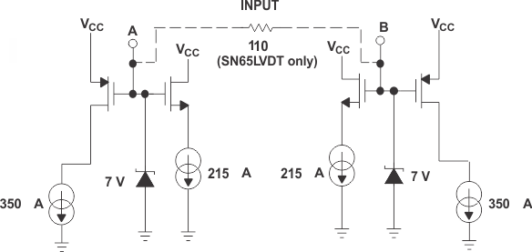 Figure 38. Receiver Equivalent Schematic
10.3.2 Driver Features
10.3.2.1 Signaling Rate, Edge Rate, and Added Jitter
The SN65LVDT10x family has been designed to provide uncompromising signal quality at signaling rates up to 2 Gbps, and beyond. Specifying a maximum signaling rate (the signaling rate is the same as the bit rate) for a device depends on the eye quality that can be achieved. This eye quality is driven by a number of factors, with two of the most critical parameters being the rise or fall time and added jitter.
The rise and fall times for a device are critical for an obvious reason: the time it takes for a device to change states will be a limiting factor in how fast a device can be operated. If a device is operated much faster than the speed at which it can change states, the vertical opening of the eye diagram will be decreased. In some cases this may be perfectly acceptable. As an example, assume an SN65LVDS100 is being using to receive a CML signal, and translate the CML signal into an LVDS signal. At speeds up to 2 Gbps (or 1 GHz for a clock signal because there are 2 bit times for each clock cycle), the LVDS output signal will have a differential output voltage of at least 247 mV, with a nominal value of 340 mV (see the Electrical Characteristics section for reference). If the input is at a higher speed, there is no circuitry within the SN65LVDS100 that would prevent the device from trying to output an LVDS signal. As the signaling rate is increased beyond 2 Gbps, the output signal would show a decrease in vertical eye opening. This decrease may not impact the utility of the device at the system level. Signal chain noise analysis would need to be performed to determine whether the overall system would be affected.
In a similar way, we can see the effect of added jitter, and how it can place upper limits on the useful operating rate. At the stated 2-Gbps signaling rate, the unit interval (UI) time, tUI, is the reciprocal of 2 Gbps, or 500 ps. As added jitter is introduced by a device such as the SN65LVDT10x family, it serves to close down the eye pattern horizontally (or in time). As the output eye diagram will eventually be used to recover the transmitted or encoded data, the jitter tolerance at the eventual consumer would determine if the eye closure introduced by a SN65LVDT10x is acceptable. The nominal total jitter for the SN65LVDT10x family devices is 28 ps, while the worst case jitter is 65 ps. The 28 ps represents less than 6% of the UI and the 65 ps represents 13% of the UI. Both values will generally be within the amount of added jitter that can be tolerated in a system.
10.3.2.2 SN65LVDx100 LVDS Output
10.3.2.2.1 Driver Output Voltage
The SN65LVDx100 driver operates and meets all the specified performance requirements for supply voltages in the range of 3 V to 3.6 V. The driver output voltage has a nominal value of 340 mV, with maximum and minimum output voltages that meet the LVDS standard specifications of 247 mV and 454 mV, respectively.
10.3.2.2.2 Driver Offset
An LVDS compliant driver is required to maintain the common-mode output voltage at 1.2 V (±75 mV). The SN65LVDx100 incorporates sense circuitry and a control loop to source common-mode current and keep the output signal within specified values. Further, the device maintains the output common-mode voltage at this set point over the full 3-V to 3.6-V supply range.
10.3.2.3 SN65LVDx101 LVPECL Output
10.3.2.3.1 Driver Voltage
The SN65LVDx101 driver is an LVPECL differential driver. Figure 40 shows an equivalent output schematic for the SN65LVDx101 driver. The differential signal output of the driver is simply the output of the differential pair, emitter-coupled to the device output. For an ECL class device such as this, the output base-emitter diodes must always be on. This need for the consistently active output stages helps explain the classical ECL load shown in Figure 39.
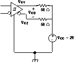 Figure 39. Typical Termination for LVPECL Output Driver (SN65LVDx101)
Figure 39 shows that the SN65LVDx101 outputs drive 50-Ω loads terminated to a supply that is 2 V below the supply voltage of the SN65LVDx101 device. Driving a load that is referenced to a supply 2 V below the device supply assures that the final transistor stages in the output driver are always on. A common question for those new to ECL devices concerns the implementation of this output load. There is no need generally to have a regulated supply to support this. A Thevenin load is often used to create a 50-Ω effective termination, at a common-mode voltage 2 V below the local supply rail. Many other implementations have been used. The key to the specific load that is implemented lies in the understanding that the ECL driver output stage is a voltage driver, with the output voltage always referenced to the positive power rail for the device. The load that is driven must ensure that the final transistors on each output leg are in the active regions at all times.
10.3.2.4 Driver Equivalent Schematics
The SN65LVDx10x equivalent output schematic diagrams are shown in Figure 40. The SN65LVDx10x output is represented by a differential pair with 7-V Zener diodes on each output leg. The Zener diodes provide ESD protection. The SN65LVDx10x1 LVPECL output is represented by a differential pair, with follower stages, and with 7-V Zener diodes on each output leg for ESD protection.
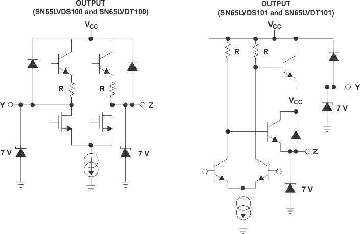 Figure 40. Driver Equivalent Schematics
10.4 Device Functional Modes
Table 2. SN65LVDx10x Truth Table
| DIFFERENTIAL INPUT | OUTPUTS(1) | |
|---|---|---|
| VID = VA – VB | Y | Z |
| VID ≥ 100 mV | H | L |
| –100 mV < VID < 100 mV | ? | ? |
| VID ≤ –100 mV | L | H |
| Open | ? | ? |