SCAS956D May 2023 – March 2024 SN74AC244-Q1
PRODUCTION DATA
- 1
- 1 Features
- 2 Applications
- 3 Description
- 4 Pin Configuration and Functions
-
5 Specifications
- 5.1 Absolute Maximum Ratings
- 5.2 ESD Ratings
- 5.3 Recommended Operating Conditions
- 5.4 Thermal Information
- 5.5 Electrical Characteristics
- 5.6 Switching Characteristics 1.5-V VCC
- 5.7 Switching Characteristics 1.8-V VCC
- 5.8 Switching Characteristics 2.5-V VCC
- 5.9 Switching Characteristics 3.3-V VCC
- 5.10 Switching Characteristics 5-V VCC
- 5.11 Noise Characteristics
- 5.12 Typical Characteristics
- 6 Parameter Measurement Information
- 7 Detailed Description
- 8 Application Information Disclaimer
- 9 Device and Documentation Support
- 10Revision History
- 11Mechanical, Packaging, and Orderable Information
Package Options
Refer to the PDF data sheet for device specific package drawings
Mechanical Data (Package|Pins)
- RKS|20
- DGS|20
- PW|20
Thermal pad, mechanical data (Package|Pins)
- RKS|20
Orderable Information
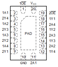
4 Pin Configuration and Functions
 Figure 4-1 RKS
Package, 20-Pin VQFN (Top View)
 Figure 4-2 DGS or PW Package, 20-Pin VSSOP or
TSSOP (Top View)
Figure 4-2 DGS or PW Package, 20-Pin VSSOP or
TSSOP (Top View)Table 4-1 Pin Functions
| PIN | TYPE(1) | DESCRIPTION | |
|---|---|---|---|
| NAME | NO. | ||
| 1OE | 1 | I | Bank 1, output enable, active low |
| 1A1 | 2 | I | Bank 1, channel 1 input |
| 2Y4 | 3 | O | Bank 2, channel 4 output |
| 1A2 | 4 | I | Bank 1, channel 2 input |
| 2Y3 | 5 | O | Bank 2, channel 3 output |
| 1A3 | 6 | I | Bank 1, channel 3 input |
| 2Y2 | 7 | O | Bank 2, channel 2 output |
| 1A4 | 8 | I | Bank 1, channel 4 input |
| 2Y1 | 9 | O | Bank 2, channel 1 output |
| GND | 10 |
G |
Ground |
| 2A1 | 11 | I | Bank 2, channel 1 input |
| 1Y4 | 12 | O | Bank 1, channel 4 output |
| 2A2 | 13 | I | Bank 2, channel 2 input |
| 1Y3 | 14 | O | Bank 1, channel 3 output |
| 2A3 | 15 | I | Bank 2, channel 3 input |
| 1Y2 | 16 | O | Bank 1, channel 2 output |
| 2A4 | 17 | I | Bank 2, channel 4 input |
| 1Y1 | 18 | O | Bank 1, channel 1 output |
| 2OE | 19 | I | Bank 2, output enable, active low |
| VCC | 20 |
P |
Positive supply |
| Thermal pad(2) | — | The thermal pad can be connected to GND or left floating. Do not connect to any other signal or supply | |
(1) I = input, O = output, I/O = input or output, G
= ground, P = power.
(2) RKS package
only.