SCES591J JULY 2004 – June 2014 SN74AUP1G07
PRODUCTION DATA.
- 1 Features
- 2 Applications
- 3 Description
- 4 Simplified Schematic
- 5 Revision History
- 6 Pin Configuration and Functions
-
7 Specifications
- 7.1 Absolute Maximum Ratings
- 7.2 Handling Ratings
- 7.3 Recommended Operating Conditions
- 7.4 Thermal Information
- 7.5 Electrical Characteristics
- 7.6 Switching Characteristics, CL = 5 pF
- 7.7 Switching Characteristics, CL = 10 pF
- 7.8 Switching Characteristics, CL = 15 pF
- 7.9 Switching Characteristics, CL = 30 pF
- 7.10 Operating Characteristics
- 7.11 Typical Characteristics
- 8 Parameter Measurement Information
- 9 Detailed Description
- 10Application and Implementation
- 11Power Supply Recommendations
- 12Layout
- 13Device and Documentation Support
- 14Mechanical, Packaging, and Orderable Information
10 Application and Implementation
10.1 Application Information
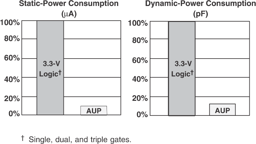
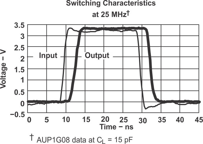
The AUP family is TI's premier solution to the industry’s low-power needs in battery-powered portable applications. This family ensures a very low static and dynamic power consumption across the entire VCC range of 0.8 V to 3.6 V, resulting in an increased battery life. This product also maintains excellent signal integrity. It has a small amount of hysteresis built in allowing for slower or noisy input signals. The lowered drive produces slower edges and prevents overshoot and undershoot on the outputs.
10.2 Typical Application
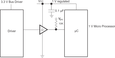 Figure 5. Typical Application Schematic
10.2.1 Design Requirements
This device uses CMOS technology and has balanced output drive. Care should be taken to avoid bus contention because it can drive currents that would exceed maximum limits.
10.2.2 Detailed Design Procedure
- Recommended Input conditions
- Rise time and fall time specs. See (Δt/ΔV) in Recommended Operating Conditions
- Specified high and low levels. See (VIH and VIL) in Recommended Operating Conditions
- Inputs are overvoltage tolerant allowing them to go as high as 3.6 V at any valid VCC
- Recommend output conditions
- Load currents should not exceed 20 mA on the output and 50 mA total for the part
10.2.3 Application Curves
The AUP family of single gate logic makes excellent translators for the new lower voltage microprocessors that typically are powered from 0.8 V to 1.2 V. They can drop the voltage of peripheral drivers and accessories that are still powered by 3.3 V to the new uC power levels.