SCDS003P November 1992 – December 2015 SN74CBT3383
- 1 Features
- 2 Applications
- 3 Description
- 4 Revision History
- 5 Pin Configuration and Functions
- 6 Specifications
- 7 Parameter Measurement Information
- 8 Detailed Description
- 9 Application and Implementation
- 10Power Supply Recommendations
- 11Layout
- 12Device and Documentation Support
- 13Mechanical, Packaging, and Orderable Information
Package Options
Refer to the PDF data sheet for device specific package drawings
Mechanical Data (Package|Pins)
- DBQ|24
- DB|24
- DW|24
- PW|24
Thermal pad, mechanical data (Package|Pins)
Orderable Information
1 Features
- High-Bandwidth Data Path (Up to 200 MHz)
- Low and Flat ON-State Resistance (rON) Characteristics Over Operating Range
(rON = 5 Ω Typical) - Control Inputs Can Be Driven by TTL or 5-V and 3.3-V CMOS Outputs
- Bidirectional Data Flow With Near-Zero Propagation Delay
- Low Input and Output Capacitance Minimizes Loading and Signal Distortion (Cio(OFF) = 6 pF Typical)
- VCC Operating Range From 4.5 V to 5 V
- Low Power Consumption (ICC = 50 µA Maximum)
2 Applications
- Enterprise Servers
- Ethernet Switches
- Routers
- Servers
- Industrial PCs
3 Description
The SN74CBT3383 and SN54CBT3383 devices provide ten bits of high-speed TTL-compatible bus switching or exchanging. The low ON-state resistance of the switch allows connections to be made with minimal propagation delay.
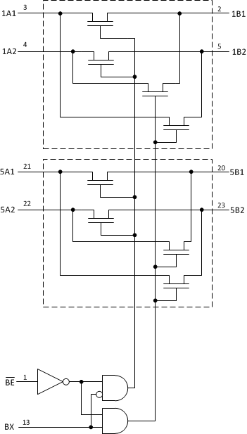
The devices operate as a 10-bit bus switch or a 5-bit bus exchanger, which provides swapping of the A and B pairs of signals. The bus-exchange function is selected when BX is high. The switches are connected when BE is low.
Device Information(1)
| PART NUMBER | PACKAGE | BODY SIZE (NOM) |
|---|---|---|
| SN74CBT3383DB | SSOP (24) | 8.40 mm × 5.30 mm |
| SN74CBT3383DBQ | SSOP (24) | 8.65 mm × 3.90 mm |
| SN74CBT3383DW | SOIC (24) | 15.40 mm × 7.50 mm |
| SN74CBT3383PW | TSSOP (24) | 7.80 mm × 4.40 mm |
| SNJ54CBT3383JT | CDIP (24) | 32.00 mm × 6.92 mm |
| SN54CBT3383W | CFP (24) | 14.35 × 9.08 mm |
- For all available packages, see the orderable addendum at the end of the data sheet.
Logic Diagram (Positive Logic)
