SCDS003P November 1992 – December 2015 SN74CBT3383
- 1 Features
- 2 Applications
- 3 Description
- 4 Revision History
- 5 Pin Configuration and Functions
- 6 Specifications
- 7 Parameter Measurement Information
- 8 Detailed Description
- 9 Application and Implementation
- 10Power Supply Recommendations
- 11Layout
- 12Device and Documentation Support
- 13Mechanical, Packaging, and Orderable Information
Package Options
Refer to the PDF data sheet for device specific package drawings
Mechanical Data (Package|Pins)
- DBQ|24
- DB|24
- DW|24
- PW|24
Thermal pad, mechanical data (Package|Pins)
Orderable Information
8 Detailed Description
8.1 Overview
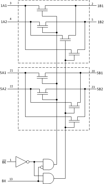
The SNX4CBT3383 provides ten high-speed CMOS TTL-compatible bus switches. The low ON-resistance of the SNX4CBT3383 allows inputs to be connected to outputs without adding propagation delay and without generating additional ground bounce noise. The Bus Enable (BE) signal turns the switches on. The Bus Exchange (BX) signal provides nibble swap of the 1A and 1B pairs of signals. This exchange configuration allows byte swapping of buses in systems. It can also be used as a 5-wide, 2-to-1 multiplexer, to create low delay barrel shifters, and so forth.
8.2 Functional Block Diagram

8.3 Feature Description
8.3.1 Bidirectional Data Flow With Near-Zero Propagation Delay
The SN74CBT3383 features a low propagation delay or tpd that works great for multiple rail information transfer from 1A1to 1B1 and 1A2 to 1B2 for example. However, the SNX4CBT3383 also features BUS exchange functionality, which allows for bidirectional data transfers from the inputs and outputs connected on the B side. By enabling the BX pin, the outputs are now crossed, or exchanged, and data can now flow from 1A1 to 1B2 and 1A2 to 1B1 with little to no propagation delay. This can be used to enable byte swapping of buses within a system or to create a 5-wide, 2-to-1 multiplexer.
8.4 Device Functional Modes
Table 1 lists the functional modes of the SNx4CBT3383.
Table 1. Function Table
| INPUTS | INPUTS / OUTPUT | ||
|---|---|---|---|
| BE | BX | 1A1-5A1 | 1A2-5A2 |
| L | L | 1B1-5B1 | 1B2-5B2 |
| L | H | 1B2-5B2 | 1B1-5B1 |
| H | X | Z | Z |