SCLS077F March   1984  – April 2021 SN54HC03 , SN74HC03

PRODUCTION DATA  

  1. Features
  2. Applications
  3. Description
  4. Revision History
    1.     Pin Configuration and Functions
      1.      Pin Functions
  5. Specifications
    1. 5.1 Absolute Maximum Ratings
    2. 5.2 Recommended Operating Conditions
    3. 5.3 Thermal Information
    4. 5.4 Electrical Characteristics - 74
    5. 5.5 Electrical Characteristics - 54
    6. 5.6 Switching Characteristics - 54
    7. 5.7 Switching Characteristics - 74
    8. 5.8 Operating Characteristics
    9. 5.9 Typical Characteristics
  6. Parameter Measurement Information
  7. Detailed Description
    1. 7.1 Overview
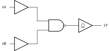
    2. 7.2 Functional Block Diagram
    3. 7.3 Feature Description
      1. 7.3.1 CMOS Open-Drain Outputs
      2. 7.3.2 Standard CMOS Inputs
      3. 7.3.3 Clamp Diode Structure
    4. 7.4 Device Functional Modes
  8. Application and Implementation
    1. 8.1 Application Information
    2. 8.2 Typical Application
      1. 8.2.1 Design Requirements
        1. 8.2.1.1 Power Considerations
        2. 8.2.1.2 Input Considerations
        3. 8.2.1.3 Output Considerations
      2. 8.2.2 Detailed Design Procedure
      3. 8.2.3 Application Curves
  9. Power Supply Recommendations
  10. 10Layout
    1. 10.1 Layout Guidelines
    2. 10.2 Layout Example
  11. 11Device and Documentation Support
    1. 11.1 Documentation Support
      1. 11.1.1 Related Documentation
    2. 11.2 Related Links
    3. 11.3 Support Resources
    4. 11.4 Trademarks
    5. 11.5 Electrostatic Discharge Caution
    6. 11.6 Glossary
  12. 12Mechanical, Packaging, and Orderable Information

Package Options

Refer to the PDF data sheet for device specific package drawings

Mechanical Data (Package|Pins)
  • D|14
  • PW|14
  • N|14
  • NS|14
Thermal pad, mechanical data (Package|Pins)
Orderable Information

Functional Block Diagram

GUID-8148A739-8C6B-4AA6-A749-E028DB6E1740-low.gif