SCLS115G December 1982 – September 2015 SN54HC164 , SN74HC164
PRODUCTION DATA.
- 1 Features
- 2 Applications
- 3 Description
- 4 Revision History
- 5 Device Comparison Table
- 6 Pin Configuration and Functions
-
7 Specifications
- 7.1 Absolute Maximum Ratings
- 7.2 ESD Ratings
- 7.3 Recommended Operating Conditions
- 7.4 Thermal Information
- 7.5 Electrical Characteristics, TA = 25°C
- 7.6 Electrical Characteristics, TA = -55°C to 125°C
- 7.7 Electrical Characteristics, TA = -55°C to 85°C
- 7.8 Timing Requirements, TA = 25°C
- 7.9 Timing Requirements, TA = -55°C to 125°C
- 7.10 Timing Requirements, TA = -55°C to 85°C
- 7.11 Switching Characteristics, TA = 25°C
- 7.12 Switching Characteristics, TA = -55°C to 125°C
- 7.13 Switching Characteristics, TA = -55°C to 85°C
- 8 Parameter Measurement Information
- 9 Detailed Description
- 10Application and Implementation
- 11Power Supply Recommendations
- 12Layout
- 13Device and Documentation Support
- 14Mechanical, Packaging, and Orderable Information
Package Options
Refer to the PDF data sheet for device specific package drawings
Mechanical Data (Package|Pins)
- D|14
- PW|14
- N|14
- NS|14
Thermal pad, mechanical data (Package|Pins)
Orderable Information
10 Application and Implementation
10.1 Application Information
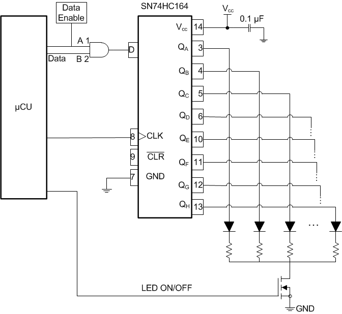
The SNx4HC164 is an 8-bit shift register that can be used as a deserializer in order to reduce the number of GPIO's needed when driving multiple LED's. In order to correctly display the proper output in the LED's a sink MOSFET was added to prevent the LED's from lighting up until the correct data or the proper clock signal has been achieved.
10.2 Typical Application
 Figure 4. Typical Application Diagram
10.2.1 Design Requirements
Ensure that the incoming clock rising edge meets the criteria in Recommended Operating Conditions.
10.2.2 Detailed Design Procedure
Ensure that input and output voltages do not exceed ratings in Absolute Maximum Ratings.
Input voltage threshold information can be found in Recommended Operating Conditions.
Detailed timing requirements can be found in Timing Requirements, TA = 25°C.
10.2.3 Application Curve
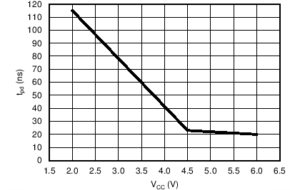
 Figure 5. Propagation Delay vs Supply Voltage at TA = 25°C