SCLS116H December 1982 – December 2015 SN54HC165 , SN74HC165
PRODUCTION DATA.
- 1 Features
- 2 Applications
- 3 Description
- 4 Revision History
- 5 Pin Configuration and Functions
-
6 Specifications
- 6.1 Absolute Maximum Ratings
- 6.2 ESD Ratings
- 6.3 Recommended Operating Conditions
- 6.4 Thermal Information
- 6.5 Electrical Characteristics, TA = 25°C
- 6.6 Electrical Characteristics, SN54HC165
- 6.7 Electrical Characteristics, SN74HC165
- 6.8 Switching Characteristics, TA = 25°C
- 6.9 Switching Characteristics, SN54HC165
- 6.10 Switching Characteristics, SN74HC165
- 6.11 Timing Requirements, TA = 25°C
- 6.12 Timing Requirements, SN54HC165
- 6.13 Timing Requirements, SN74HC165
- 6.14 Operating Characteristics
- 6.15 Typical Characteristics
- 7 Parameter Measurement Information
- 8 Detailed Description
- 9 Application and Implementation
- 10Power Supply Recommendations
- 11Layout
- 12Device and Documentation Support
- 13Mechanical, Packaging, and Orderable Information
Package Options
Refer to the PDF data sheet for device specific package drawings
Mechanical Data (Package|Pins)
- DB|16
- PW|16
- NS|16
- N|16
- D|16
Thermal pad, mechanical data (Package|Pins)
Orderable Information
1 Features
- Wide Operating Voltage Range of 2 V to 6 V
- Outputs Can Drive Up to 10 LSTTL Loads
- Low Power Consumption, 80-µA Maximum ICC
- Typical tpd = 13 ns
- ±4-mA Output Drive at 5 V
- Low Input Current of 1 µA Maximum
- Complementary Outputs
- Direct Overriding Load (Data) Inputs
- Gated Clock Inputs
- Parallel-to-Serial Data Conversion
-
On Products Compliant to MIL-PRF-38535,
All Parameters Are Tested Unless Otherwise Noted. On All Other Products, Production Processing Does Not Necessarily Include Testing of All Parameters.
2 Applications
- Programable Logic Controllers
- Appliances
- Video Display Systems
- Output Expander
- Keyboards
3 Description
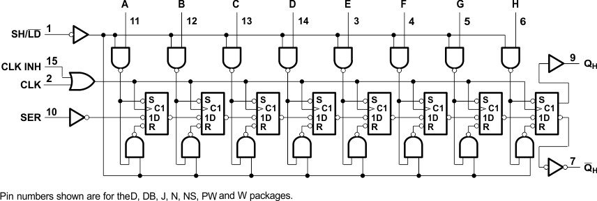
The SNx4HC165 devices are 8-bit parallel-load shift registers that, when clocked, shift the data toward a serial (QH) output. Parallel-in access to each stage is provided by eight individual direct data (A−H) inputs that are enabled by a low level at the shift/load (SH/LD) input. The SNx4HC165 devices also feature a clock-inhibit (CLK INH) function and a complementary serial (QH) output.
Clocking is accomplished by a low-to-high transition of the clock (CLK) input while SH/LD is held high and CLK INH is held low. The functions of CLK and CLK INH are interchangeable. Because a low CLK and a low-to-high transition of CLK INH also accomplish clocking, CLK INH must be changed to the high level only while CLK is high. Parallel loading is inhibited when SH/LD is held high. While SH/LD is low, the parallel inputs to the register are enabled independently of the levels of the CLK, CLK INH, or serial (SER) inputs.
Device Information(1)
| PART NUMBER | PACKAGE | BODY SIZE (NOM) |
|---|---|---|
| SN74HC165D | SOIC (16) | 10.00 mm × 6.20 mm |
| SN74HC165DB | SSOP (16) | 8.20 mm × 6.50 mm |
| SN74HC165N | PDIP (16) | 6.60 mm × 18.92 mm |
| SN74HC165NS | SO (16) | 8.20 mm × 9.90 mm |
| SN74HC165PW | TSSOP (16) | 6.60 mm × 5.10 mm |
| SN54HC165FK | LCCC (20) | 9.09 mm × 9.09 mm |
| SN54HC165J | CDIP (16) | 21.34 mm × 7.52 mm |
| SN54HC165W | CFP (16) | 9.40 mm × 7.75 mm |
- For all available packages, see the orderable addendum at the end of the data sheet.
Logic Diagram Positive Logic
