SCLS116H December 1982 – December 2015 SN54HC165 , SN74HC165
PRODUCTION DATA.
- 1 Features
- 2 Applications
- 3 Description
- 4 Revision History
- 5 Pin Configuration and Functions
-
6 Specifications
- 6.1 Absolute Maximum Ratings
- 6.2 ESD Ratings
- 6.3 Recommended Operating Conditions
- 6.4 Thermal Information
- 6.5 Electrical Characteristics, TA = 25°C
- 6.6 Electrical Characteristics, SN54HC165
- 6.7 Electrical Characteristics, SN74HC165
- 6.8 Switching Characteristics, TA = 25°C
- 6.9 Switching Characteristics, SN54HC165
- 6.10 Switching Characteristics, SN74HC165
- 6.11 Timing Requirements, TA = 25°C
- 6.12 Timing Requirements, SN54HC165
- 6.13 Timing Requirements, SN74HC165
- 6.14 Operating Characteristics
- 6.15 Typical Characteristics
- 7 Parameter Measurement Information
- 8 Detailed Description
- 9 Application and Implementation
- 10Power Supply Recommendations
- 11Layout
- 12Device and Documentation Support
- 13Mechanical, Packaging, and Orderable Information
Package Options
Refer to the PDF data sheet for device specific package drawings
Mechanical Data (Package|Pins)
- DB|16
- PW|16
- NS|16
- N|16
- D|16
Thermal pad, mechanical data (Package|Pins)
Orderable Information
9 Application and Implementation
NOTE
Information in the following applications sections is not part of the TI component specification, and TI does not warrant its accuracy or completeness. TI’s customers are responsible for determining suitability of components for their purposes. Customers should validate and test their design implementation to confirm system functionality.
9.1 Application Information
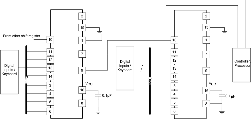
The SNx4HC165 is an 8-bit shift register that can be used as a serializer in order to reduce the number of connection needed when transmitting signals between boards or to the device. SNx4HC165 can be used to expand inputs for processors with limited GPIOs for examples basic keyboard interface to the controller. SNx4HC165 allows inputs to be load into the shift registers and clock is used to shift data to the processor. Multiple SNx4HC165 can be cascaded together to allow more digital inputs to be interfaced with single processor by connecting output of the cascaded shift register QH to serial input SER of the SNx4HC165 and so on. Note this application does not allow the communication to be bi-direction in nature as data can only be read by the processor not written back.
9.2 Typical Application
 Figure 5. Typical Application Diagram for SN74HC165
9.2.1 Design Requirements
Ensure that the incoming clock rising edge meets the criteria in Recommended Operating Conditions.
9.2.2 Detailed Design Procedure
Ensure that input and output voltages do not exceed ratings in Absolute Maximum Ratings.
Input voltage threshold information for each device can be found in the Electrical Characteristics tables in the Specifications section.
Detailed timing requirements for each device can be found in Timing Requirements tables in the Specifications section.
9.2.3 Application Curve
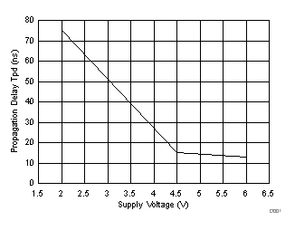
 Figure 6. Propagation Delay vs Supply Voltage at TA = 25°C