SCLS751 March 2016 SN74HC595B
PRODUCTION DATA.
- 1 Features
- 2 Applications
- 3 Description
- 4 Pin Configuration and Functions
- 5 Specifications
- 6 Parameter Measurement Information
- 7 Detailed Description
- 8 Application and Implementation
- 9 Power Supply Recommendations
- 10Layout
- 11Device and Documentation Support
- 12Mechanical, Packaging, and Orderable Information
Package Options
Mechanical Data (Package|Pins)
- RWN|16
Thermal pad, mechanical data (Package|Pins)
Orderable Information
1 Features
- 8-Bit Serial-In, Parallel-Out Shift Registers
- Available in Ultra Small Logic QFN package(0.5 mm max height)
- Over-Voltage Tolerant on Inputs Independent of Vcc
- Wide Operating Voltage Range of 2 V to 6 V
- High-Current 3-State Outputs Can Drive Up to 15 LSTTL Loads
- Low Power Consumption: 80-μA (Maximum) ICC
- tpd = 13 ns (Typical)
- ±6-mA Output Drive at 5 V
- Low Input Current: 1 μA (Maximum)
- Shift Register Has Direct Clear
- -55oC to 125oC Operating Temperature
2 Applications
- Network Switches
- Factory Automation
- Mobile Wearables
- Industrial Building Automation
- Power Infrastructure
- LED Displays
- Servers
3 Description
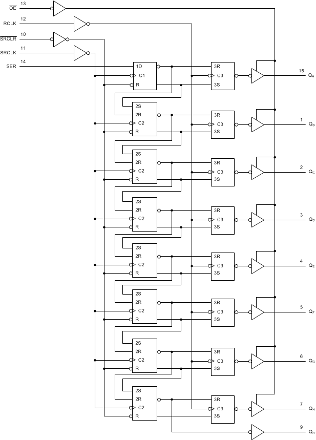
The SN74HC595B devices contain an 8-bit, serial-in, parallel-out shift register that feeds an 8-bit D-type storage register. The storage register has parallel 3-state outputs. Separate clocks are provided for both the shift register and storage register. The shift register has a direct overriding clear (SRCLR) input, serial (SER) input, and serial outputs for cascading. When the output-enable (OE) input is high, the all outputs are in the high-impedance state except QH'.
Table 1. Device Information
| PART NUMBER | PACKAGE (PINS) | BODY SIZE (NOM) |
|---|---|---|
| SN74HC595BRWN | X1QFN (16) | 2.50 mm x 2.50 mm |
- For available package, see the orderable addendum at the end of the data sheet.
Logic Diagram (Positive Logic)
