SCLS751 March 2016 SN74HC595B
PRODUCTION DATA.
- 1 Features
- 2 Applications
- 3 Description
- 4 Pin Configuration and Functions
- 5 Specifications
- 6 Parameter Measurement Information
- 7 Detailed Description
- 8 Application and Implementation
- 9 Power Supply Recommendations
- 10Layout
- 11Device and Documentation Support
- 12Mechanical, Packaging, and Orderable Information
Package Options
Mechanical Data (Package|Pins)
- RWN|16
Thermal pad, mechanical data (Package|Pins)
Orderable Information
7 Detailed Description
7.1 Overview
The SN74HC595B is part of the HC family of logic devices intended for CMOS applications. The SN74HC595B device is an 8-bit shift register that feeds an 8-bit D-type storage register.
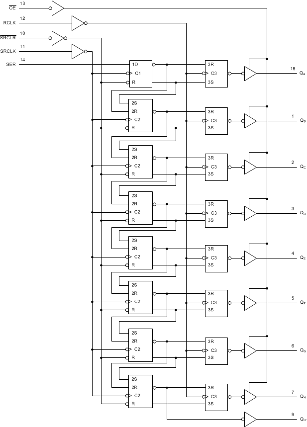
Both the shift register clock (SRCLK) and storage register clock (RCLK) are positive-edge triggered. If both clocks are connected together, the shift register is always one clock pulse ahead of the storage register. The QH' may be used for daisy chaining the device and will not go into high impedance when OE is asserted.
7.2 Functional Block Diagram
 Figure 4. Logic Diagram (Positive Logic)
7.3 Feature Description
The SN74HC595B device is an 8-bit Serial-In, Parallel-Out shift register. It has a wide operating voltage of 2 V to 6 V, and the high-current 3-state outputs can drive up to 15 LSTTL Loads. The device has a low power consumption of 80-μA (Maximum) ICC. Additionally, this device has a low input current of 1 μA (Maximum) and a ±6-mA output drive at 5 V. The device is available currently in the smallest logic QFN package at 0.5 mm max height with 0.4 mm pitch. The inputs are over voltage tolerant independent of Vcc.
7.4 Device Functional Modes
Table 3 lists the functional modes of the SN74HC595B devices.
Table 3. Function Table
| INPUTS | FUNCTION | ||||
|---|---|---|---|---|---|
| SER | SRCLK | SRCLR | RCLK | OE | |
| – | – | – | – | H | Outputs QA – QH are disabled. QH' is active . |
| – | – | – | – | L | Outputs QA – QH are enabled. |
| – | – | L | – | – | Shift register is cleared. |
| L | ↑ | H | – | – | First stage of the shift register goes low. Other stages store the data of previous stage, respectively. |
| H | ↑ | H | – | – | First stage of the shift register goes high. Other stages store the data of previous stage, respectively. |
| – | – | – | ↑ | – | Shift-register data is stored in the storage register. |