SCLS880A October   2021  – December 2021 SN74HCT595

PRODUCTION DATA  

  1. Features
  2. Applications
  3. Description
  4. Revision History
  5. Pin Configuration and Functions
  6. Specifications
    1. 6.1 Absolute Maximum Ratings
    2. 6.2 ESD Ratings
    3. 6.3 Recommended Operating Conditions
    4. 6.4 Thermal Information
    5. 6.5 Electrical Characteristics
    6. 6.6 Timing Characteristics
    7. 6.7 Switching Characteristics
    8.     14
    9. 6.8 Typical Characteristics
  7. Parameter Measurement Information
  8. Detailed Description
    1. 8.1 Functional Block Diagram
    2. 8.2 Feature Description
      1. 8.2.1 Balanced CMOS 3-State Outputs
      2. 8.2.2 Balanced CMOS Push-Pull Outputs
      3. 8.2.3 TTL-Compatible CMOS Inputs
      4. 8.2.4 Latching Logic
      5. 8.2.5 Clamp Diode Structure
    3. 8.3 Device Functional Modes
  9. Application and Implementation
    1. 9.1 Application Information
    2. 9.2 Typical Application
      1. 9.2.1 Design Requirements
        1. 9.2.1.1 Power Considerations
        2. 9.2.1.2 Input Considerations
        3. 9.2.1.3 Output Considerations
      2. 9.2.2 Detailed Design Procedure
      3. 9.2.3 Application Curve
  10. 10Power Supply Recommendations
  11. 11Layout
    1. 11.1 Layout Guidelines
    2. 11.2 Layout Example
  12. 12Device and Documentation Support
    1. 12.1 Documentation Support
      1. 12.1.1 Related Documentation
    2. 12.2 Receiving Notification of Documentation Updates
    3. 12.3 Support Resources
    4. 12.4 Trademarks
    5. 12.5 Electrostatic Discharge Caution
    6. 12.6 Glossary
  13. 13Mechanical, Packaging, and Orderable Information

Package Options

Mechanical Data (Package|Pins)
Thermal pad, mechanical data (Package|Pins)
Orderable Information

Description

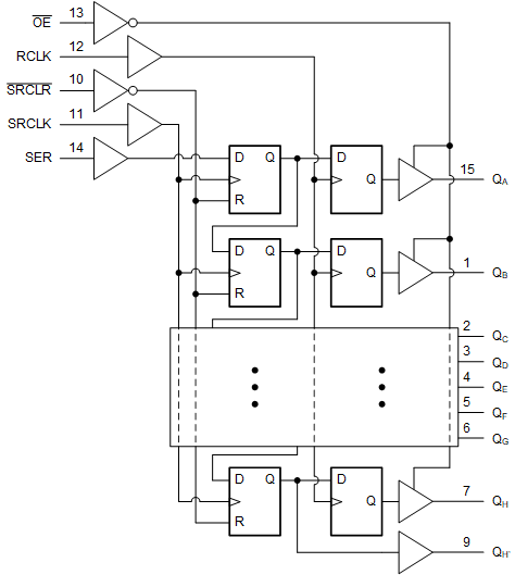
The SN74HCT595 device contains an 8-bit, serial-in, parallel-out shift register that feeds an 8-bit D-type storage register. The storage register has parallel 3-state outputs. Separate clocks are provided for both the shift and storage register. The shift register has a direct overriding clear (SRCLR) input, serial (SER) input, and a serial output (QH') for cascading. When the output-enable (OE) input is high, the storage register outputs are in a high-impedance state. Internal register data and serial output (QH') are not impacted by the operation of the OE input.

Device Information(1)
PART NUMBERPACKAGEBODY SIZE (NOM)
SN74HCT595PWTSSOP (16)5.00 mm × 4.40 mm
For all available packages, see the orderable addendum at the end of the data sheet.
GUID-20211015-SS0I-66P0-J2PR-6DVV9SDRTXZD-low.gif Logic Diagram (Positive Logic)