SDLS153A January 1981 – January 2016 SN74LS292 , SN74LS294
PRODUCTION DATA.
- 1 Features
- 2 Applications
- 3 Description
- 4 Revision History
- 5 Pin Configuration and Functions
- 6 Specifications
- 7 Parameter Measurement Information
- 8 Detailed Description
- 9 Application and Implementation
- 10Power Supply Recommendations
- 11Layout
- 12Device and Documentation Support
- 13Mechanical, Packaging, and Orderable Information
Package Options
Mechanical Data (Package|Pins)
- N|16
Thermal pad, mechanical data (Package|Pins)
Orderable Information
6 Specifications
6.1 Absolute Maximum Ratings
over operating free-air temperature range (unless otherwise noted)(1)| MIN | MAX | UNIT | ||
|---|---|---|---|---|
| VCC(2) | Supply voltage | 7 | V | |
| Input voltage | 7 | V | ||
| TJ | Junction temperature | 150 | °C | |
| Tstg | Storage temperature | –65 | 150 | °C |
(1) Stresses beyond those listed under Absolute Maximum Ratings may cause permanent damage to the device. These are stress ratings only, which do not imply functional operation of the device at these or any other conditions beyond those indicated under Recommended Operating Conditions. Exposure to absolute-maximum-rated conditions for extended periods may affect device reliability.
(2) Voltage values are with respect to network ground terminal.
6.2 Recommended Operating Conditions
over operating free-air temperature range (unless otherwise noted)| MIN | NOM | MAX | UNIT | |||
|---|---|---|---|---|---|---|
| VCC | Supply voltage | 4.75 | 5 | 5.25 | V | |
| VIH | High-level input voltage | 2 | V | |||
| VIL | Low-level input voltage | 0.8 | V | |||
| IOH | High-level output current (Q only) | –1.2 | mA | |||
| IOL | Low-level output current (Q only) | 24 | mA | |||
| fclock | Clock frequency | 0 | 30 | MHz | ||
| tw | Duration of clock input pulse | 16 | ns | |||
| tw | Duration of clear pulse | SN74LS292 | 55 | ns | ||
| SN74LS294 | 35 | |||||
| tsu | Clear inactive-state set-up time | 15 | ns | |||
| TA | Operating free-air temperature | 0 | 70 | °C | ||
6.3 Thermal Information
| THERMAL METRIC(1) | SN74LS292 | UNIT | |
|---|---|---|---|
| N (PDIP) | |||
| 16 PINS | |||
| RθJA | Junction-to-ambient thermal resistance | 36.8 | °C/W |
| RθJC(top) | Junction-to-case (top) thermal resistance | 22.2 | °C/W |
| RθJB | Junction-to-board thermal resistance | 17.0 | °C/W |
| ψJT | Junction-to-top characterization parameter | 7.0 | °C/W |
| ψJB | Junction-to-board characterization parameter | 16.8 | °C/W |
(1) For more information about traditional and new thermal metrics, see the Semiconductor and IC Package Thermal Metrics application report, SPRA953.
6.4 Electrical Characteristics
over operating free-air temperature range (unless otherwise noted)| PARAMETER | TEST CONDITIONS(1) | MIN | TYP(2) | MAX | UNIT | ||
|---|---|---|---|---|---|---|---|
| VIK | VCC = MIN, II = –18 mA | –1.5 | V | ||||
| VOH | Q | VCC = MIN, VIH = 2 V, IOH = –1.2 mA, VIL = MAX | 2.4 | 3.4 | V | ||
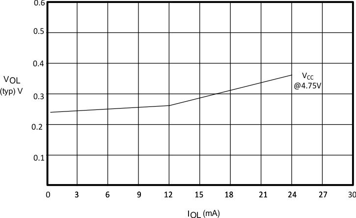
| VOL | Q | VCC = MIN, VIH = 2 V, VIL = MAX | IOL = 12 mA | 0.25 | 0.4 | V | |
| IOL = 24 mA | 0.35 | 0.5 | |||||
| TP(3) | IOL = 0.5 mA | 0.25 | 0.4 | ||||
| II | VCC = MAX, VI = 7 V | 0.1 | mA | ||||
| IIH | VCC = MAX, VI = 2.7 V | 20 | mA | ||||
| IIL | CLK1, CLK2 | VCC = MAX, VI = 0.4 V | –0.8 | mA | |||
| All others | VCC = MAX, VI = 0.4 V | –0.4 | |||||
| IOS(4) | Q | VCC = MAX | –30 | –130 | mA | ||
| ICC | SN74LS292 | VCC = MAX, all inputs grounded, all outputs open | 40 | 75 | mA | ||
| SN74LS294 | VCC = MAX, all inputs grounded, all outputs open | 30 | 50 | ||||
(1) For conditions shown as MIN or MAX, use the appropriate value specified under Recommended Operating Conditions.
(2) All typical values are at VCC = 5 V, TA = 25°C.
(3) The TP output or outputs are not intended to drive external loads, but are solely provided for test points.
(4) The duration of the short-circuit should not exceed one second.
6.5 Switching Characteristics
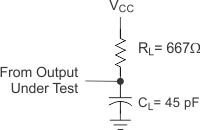
VCC = 5 V, TA = 25°C, RL = 667 Ω, CL = 45 pF (see Figure 1)| PARAMETER | TEST CONDITIONS | MIN | TYP | MAX | UNIT | ||
|---|---|---|---|---|---|---|---|
| fmax | From CLK1 or 2 | 30 | 50 | MHz | |||
| tPLH | From CLK1 or 2, to Q; Modulo set at 22, A through # = LLLHL (xxxxLS292), A through D = LLHL (xxxxLS294) | 55 | 90 | ns | |||
| tPHL | From CLK1 or 2, to Q; Modulo set at 22, A through # = LLLHL (xxxxLS292), A through D = LLHL (xxxxLS294) | 80 | 120 | ns | |||
| From CLR, to Q | SN74LS292 | 85 | 130 | ||||
| SN74LS294 | 35 | 65 | |||||
 Figure 1. Switching Loads
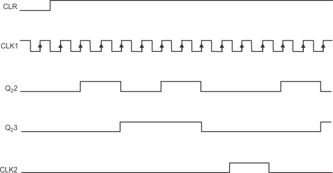
 Figure 2. Timing Diagram
6.6 Typical Characteristics
 Figure 3. VOL vs IOL